

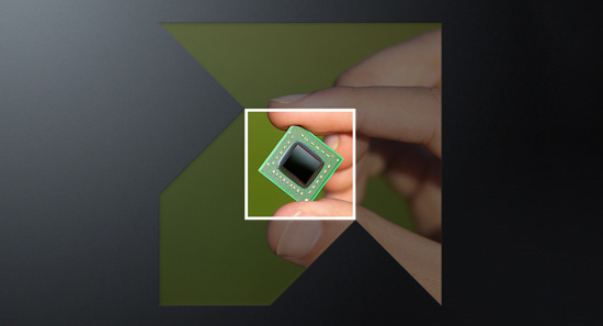
Although microprocessors based on AMD’s next-generation high-performance micro-architecture code-named “Zen” are more than a year away, some details regarding the forthcoming chips and “Zen” in general are beginning to surface. The most recent rumours about the new architecture add some technical details and point to release schedule of the new chips.
As reported, the first central processing units to use “Zen” for client PCs will be the code-named “Summit Ridge” chip that is expected to feature up to eight cores, a DDR4 memory controller, a PCI Express 3.0 controller and up to 95W thermal design power. It is projected that the chip will be made using 14nm FinFET process technology by GlobalFoundries or Samsung Electronics. Based on unofficial information, AMD’s “Summit Ridge” processors will hit the market in the third quarter of 2016.
Servers first
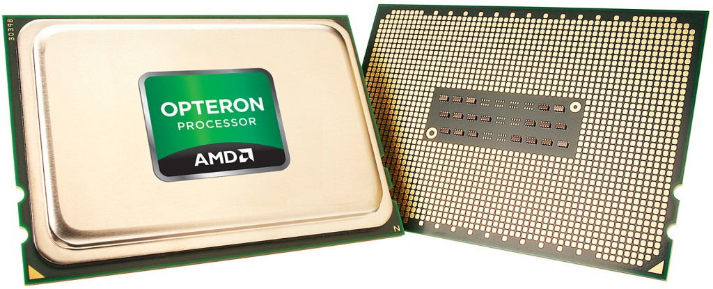
WccfTech reports citing its own sources that with “Zen” AMD will return to its traditional practice of introducing server processors powered by the latest micro-architectures first and then follow with chips for client PCs. There are no exact schedules given, but taking into account relatively slow ramp up of server processors and platforms by server makers, if AMD wants to find its new Opteron chips in 2016 servers in more or less significant quantities, it will have to introduce its new CPUs in the first half of the year.

Since eight cores inside the “Summit Ridge” are not enough for modern servers, AMD will either continue to use multi-chip-module design for Opteron processors based on “Zen” architecture next year and onwards (to get a many-core CPU out of two multi-core dies), or will make a separate multi-core design specifically for servers. In fact, AMD has had a technology to build “native” 16-core Opteron processors featuring “Bulldozer”-class dual-core modules for quite a while, but it is unknown whether it will use it even for its forthcoming chips featuring the new micro-architecture.
Keeping in mind that actual x86 cores are not large and the fact that AMD will utilize 14nm FinFET process tech (albeit with 20nm BEOL interconnect flow and hence appropriate geometries) to make “Zen”-based products, it is possible that AMD will go for native many-core design for server processors if the cores are compact enough and the company finds this a viable and cost-effective solution.
“Skylake” instructions inside “Zen” point to a new FPU
The new micro-architecture from AMD promises to be very different from the company’s current-generation “Bulldozer”-class designs, but almost nothing is known about “Zen” outside of Advanced Micro Devices at present. Without providing any details, the aforementioned media report claims that the new architecture features certain technologies found in the upcoming Intel “Skylake” processors.
Keeping in mind that AMD cannot copy Intel’s designs or even parts of it (in accordance with its x86 cross-license agreement with Intel), do not expect AMD to incorporate any of Intel’s micro-architectural know-hows into its chips. However, what AMD can do is to implement any x86/x87 extensions, enhancements as well as various new instructions introduced by Intel in its central processing units. Intel can do the same too, just like it did with x86-64 more than a decade ago. While we do not know all peculiarities of “Skylake”, many official and semi-official revelations indicate that the new micro-architecture from Intel will bring support of such technologies as AVX 3.2 (512-bit instructions), SHA extensions (SHA-1 and SHA-256, secure hash algorithms), MPX (memory protection extensions), ADX (multi-precision add-carry instruction extensions) and other innovations. AMD has rights to incorporate all of them into its micro-architectures, which it will likely do eventually.
If AMD proceeds with implementation of AVX 3.2 technology, it will have to develop a brand-new floating-point unit (FPU) to execute 512-bit instructions. At present AMD’s FPU features two 128-bit FMAC (fused multiply–add capability) pipelines that can be unified into one large 256-bit-wide unit if one of the integer cores dispatches an AVX instruction. While this approach technically works for AVX and floating-point operations (but AVX execution is dramatically slower on AMD's chips compared to Intel's chips), the AVX 2 further expands usage of most vector integer SSE and AVX instructions to 256 bits, which normally requires a new FPU. 512-bit AVX 3.2 instructions will entail further refinements of hardware, therefore, AMD’s “Zen”, if it supports AVX 3.2, will need an all-new FPU that will hardly resemble that of the “Bulldozer”. Basically, if AMD does not want to repeat the same mistakes it has done with “Bulldozer”, it will need a fully-fledged 512-bit FPU in “Zen” microprocessors. Otherwise, execution of 512-bit AVX 3.2 instructions will be awfully slow.
Summing up
The fact that AMD plans to first release Opteron chips featuring “Zen” cores and only then integrate its new cores into consumer products indicates that the company expects a lot from the micro-architecture which development is currently led by Jim Keller, a legendary CPU architect.
If AMD’s forthcoming “Zen” technology supports everything (or even the majority of) instructions introduced by Intel’s “Skylake” processors in the second half of next year, this will be a significant leap for AMD.

When it comes to performance, it is logical to expect a substantial increase of performance from AMD’s forthcoming microprocessors. At present we have no idea from where performance improvements will come from exactly. However, a new “fat” FPU in 2016 is not only a logical thing to expect, but rather a must have feature.
AMD did not comment on the news-story.
Discuss on our Facebook page, HERE.
KitGuru Says: Keep in mind that many of the things discussed here are speculations based on reports from unofficial sources. We do not know for sure that AMD plans to support AVX-512 in any form next year, we also have no idea which segments of the server market the company would like to address with its Opteron “Zen” processors first in 2016. All-in-all, take everything with a grain of salt.
‘feature up to eight cores’ is very ambiguous in AMD lingo.
True eight cores? 4 modules with 2 cores/module?
Can I assume x86-arm plan is dead?
It’s Jim Keller, it’s obviously going to have 8 full cores and look nothing at all like Bulldozer. Zen is actually one of their steps in the x86-ARM plan because they need a new architecture, and it’s probably been in development at least since they announced that, considering how long it takes to develop an architecture from scratch, so I’m not sure what you’re on.
cant remeber where but amd did say thay are droping the cluster/module design
Hey Anton Shilov
AMD OWNS x86-64 instructions and extensions. Intel does not.
Yep 😀 Formally its AMDx64 then was x86-64bit, also ATI was first on GPU Market then after 2-3 years nVidia 😉 and Yes ATI was first to implement some Teselation into their GPU’s (TrueForm) and that feature was used f.exmple in NWN 2 and other games 😀 Knowledge is POWER 😉
AMD Sky Bridge is far from dead. That is the entire reason that AMD is releasing ZEN as a server chip first. It will be socket compatible with ARM Opteron. This would give SeaMicro to ability to build to ONE hardware specification and simply plug-in ARM or x86 depending on the wishes of the client.
In fact Amur is the ARM equivalent to Nolan and is expected second half of this year.
http://wccftech.com/amds-x86-nolan-apu-fabricated-28nm-process-20nm/
There just seems to be some disagreement regarding the process node.
The other benefit could be to the tablet OEM’s building both ARM and x86 Tablets. ONE hardware build allows two different ecosystems.
Hey guys what do you think. If BLX INVEST (not buy) in AMD they will have much more money.
So do you think that FUSION is not over, and they invest in VISC architecture, they get a processor witch can do ARM and x64 at same time in One chip?
Read the cross licensing agreement: http://www.sec.gov/Archives/edgar/data/2488/000119312509236705/dex102.htm Section 3.1 and Section 3.2. This is why AMD can use MMX, SSE, SSE2, SSE4 and AVX instructions. It is also why Intel can use x64 instructions. In other words, if either party creates a new instruction set or extension, then either party is free to implement it in their chips if they want to….
Both Intel and AMD are free to use the instruction but they can not copy the architecture to do it.
MMX, SSE, SSE2, SSE4 and AVX are all Intel instructions. “SSE originally added eight new 128-bit registers known as XMM0 through XMM7. The AMD64 extensions from AMD (originally called x86-64) added a further eight registers XMM8 through XMM15, and this extension is duplicated in the Intel 64 architecture.”
http://en.wikipedia.org/wiki/Streaming_SIMD_Extensions
That’s correct, they cannot copy each other’s CPU architecture design (cache, instruction pipeline, decoders, ALUs, etc) but can use the same instruction sets. Of course there is no way AMD would copy Intel’s chip design and vice versa (Intel copying AMD’s chip designs) as that would breach chip IP patents on either sides.
Also MMX, SSE and SSE2 came before AMD’s x64. Thus still the same scenario, Intel is free to use x64 extensions (which includes the same registers used). This means AMD no longer exclusively own x64 instructions because the cross license agreement goes both ways.
That BLX was a rumour based on past collaborations with AMD particularly the usage of AMD chipsets for Longsoon CPUs as seen in Lemote products: http://en.wikipedia.org/wiki/Lemote . If that BLX investment were true then AMD would have openly/officially announce it just to prep up their depressed share prices and waning investor confidence. But officially AMD never came out and announce anything about it…
For your information, already exist an ARM CPU inside Kaveri chips used as for TrustZone function. Putting both ARM as CPU and x86 in a single chip can be messy (not recommended), especially when it comes to firmware and software.
ARM based Opteron A1100 already released but being sold by AMD as a development kit currently: http://www.amd.com/en-us/products/server/opteron-a-series And its a BGA chip (soldered on the boad) rather than a socket type. Still have zero deployments in actual servers (not even in any SeaMicro products: http://www.seamicro.com/products ). This is due to ARM’s infancy in servers especially in software and operating system ecosystem. Example: http://www.pcworld.idg.com.au/article/566539/lenovo-building-its-first-prototype-arm-server/ quotes…
“Intel today holds more than 90 percent market share in servers, and even ARM server chip vendors like AMD have admitted it may take many years before the chips are widely adopted in data centers. But an effort is underway to raise awareness about the chips’ benefits and to develop compatible software.”
Actually the instruction set known as x86-64 is AMD IP. It was developed to be backwards compatible to 32 bit legacy software while Intels IA-64 which was developed for Itanic was not. MMX, SSE, SSE2 etc are i386 instructions which many Intel and AMD cpu’s and APU’s still support.
https://gcc.gnu.org/onlinedocs/gcc-4.0.0/gcc/i386-and-x86_002d64-Options.html#i386-and-x86_002d64-Options
I don’t know what point your making but you seem to be somewhat confused regarding what is AMD IP.
Intel’s IA-64 was exclusively for Itanium CPUs, and not x86 based CPUs : http://en.wikipedia.org/wiki/IA-64 Also x64 is not really backwards compatible with 32-bit x86 instruction. It has different register size and addressing space. When running in 64-bit mode, it will not run old 32-bit mode instructions. This is why 32-bit programs will run as 32-bit only programs (or as a virtual 32-bit protected mode environment under 64-bit operating systems). It is also why you cannot use 32-bit drivers on 64-bit operating systems.
And MMX, SSE and SSE2 instructions started in the newer Pentium generations, not found on the older i386 generation. These instruction sets were created and developed by Intel to supersede the ancient x87 FPU instructions and to add SIMD capability. You can see them also in AMD chips is because of the cross license agreement. This way many x86 instructions can be standardized on the x86 platform (allowing easier software development). This is why AMD typically also implement them in their own chips.
The point is that AMD’s IP on x64 extensions exclusivity/ownership becomes irrelevant because of the cross licensing agreement since they can freely be used by Intel also. Same goes with any of Intel’s new instructions or extensions used by AMD. When Skylake introduces AVX 3.2 then AMD may also implement the same instruction set (if AMD desires)…
Then read the cross license agreement further down at Section 5 onwards. If the license becomes terminated then Intel keeps all existing instructions/extensions including AMD’s x64. Your original statement “AMD OWNS x86-64 instructions and extensions. Intel does not.” is incorrect.
Very Informative Post. Good work Kit Guru
Pls dont hate on me if I got it wrong, but the x86-64 is “just” an extension to 32bit, so extending it from 32bit to 64bit. If I remember correctly, didnt ARM(yes ARM, even though its a completely odifferent platform) design an architecture which was purely 64bit? “True” 64bit instead of an extending 32 to 64bit?
Actually the instruction sets for both 64-bit mode and 32-bit modes are not compatible. The reasons is that the register size and addressing range is different. In 32-bit mode the registers are 32-bit wide only and memory addressing limited to 4GB, while in 64-bit mode the registers are 64-bit wide and memory addressing can be greater than 4GB. Also in 64-bit mode certain memory addresses will be re-mapped differently especially GPU video RAM areas. For example, cannot use 32-bit mode’s 32-bit addressing under 64-bit mode as that can be disastrous.
You can still run 32-bit software under 64-bit operating system in a 32-bit protected mode where the CPU runs 32-bit instructions only (like a virtual 32-bit machine). But cannot run 32-bit mode instructions in 64-bit mode, and vice versa. The CPU can execute either 32-bit instructions in 32bit mode, or 64-bit instructions in 64-bit mode but not both together. If you are confused, that’s because the CPU itself can switch between 32-bit mode and 64-bit mode (under 64-bit operating systems this switching is handled by the pre-emptive scheduler).
There’s also other legacy modes including the old 16-bit 8088 instruction set (from the prehistoric IBM PC/XT era). Again, cannot use the 16-bit mode instruction in either 32-bit mode or 64-bit mode.
“Basically, if AMD does not want to repeat the same mistakes it has done
with “Bulldozer”, it will need a fully-fledged 512-bit FPU in “Zen”
microprocessors. Otherwise, execution of 512-bit AVX 3.2 instructions
will be awfully slow.”
That’s utter nonsense. You actually don’t need a 512-bit FPU in a client CPU. Vec4 double precision (== 256-bit) is enough for client apps. Most even don’t need that. For example, games (OpenGL, Direct3D) are based on single precision 3/4-way vectors. More FPU resources are waste in my opinion. That’s not a good idea on a serial high frequency compute unit. We already see with Haswell how 256-bit AVX can heat up the CPU and increases power consumption noticeably. 512-bit AVX makes it even worse.
Intel introduced 512-bit AVX only because of their Tera Scale architecture (Xeon Phi). AMD should better rely on GCN for high parallel FP throughput via OpenCL or HSA. For Zen they could recycle their Flex FPU mechanics. But this time with 256-bit FMA units. That would still be a significant uplift over Bulldozer’s 128-bit FMACs.
Actually no one cares if Skylake wins irrelevant AVX3.2 benchmarks. But people care if you win real world apps like games, browsers, audio/video transcoders, etc. And you can support AVX3.2 even with a 256-bit FPU. Look at Jaguar/Puma. It has only a 128-bit FPU and still supports AVX without “being awfully slow”.
What you are missing here is the fact that with a 512bit fpu you can run 4 128bit avx instructions in one “work cycle”
No, you can’t. Obviously you are confused about instructions and data words.
Well you kinda can, it can process sixteen 32bit integers or floats in 1 instruction. Thats 4 times the amount of data as 128bit SSE/AVX. Any app that has alot of floating point data to transform will benefit if written to support it.
One instruction is still one instruction and not four. 😉
But that’s not the point. As I said before, if you want such a high level of parallelism you better offload your data to the GPU or any other TCU. A CPU is a serial compute unit. You don’t need a beefy and power-hungry FPU in a CPU because there are a lot more integer/memory instructions per thread.
Well it depends what you’r processing.
There are times when its beneficial to use cpu processing over gpu.
1) When your GPU is busy doing other work.
2) When you need the result back with very low latency. Sending data down to the gpu, processing and getting the results back has quite a latency involved.
3) When you’re using VM’s. GPU support in VM’s is still awful, or usually unsupported. Supporting AVX-512 in VM’s is as trivial as supporting SSE.
1) Your GPU is usually busy when it renders graphics or does already a lot of FP calculations. A 512-bit FPU in the CPU is waste for such scenarios. It can’t contribute any meaningful performance.
2) Unified memory (HSA) solves this problem. You don’t need to copy the data around anymore. You simply work with pointers. Stacked memory also reduces latency a lot compared to traditional RAM.
3) A VM probably isn’t the right solution if you need high FP performance.
If the big answer is “it’s Jim Keller” expect an epic fail.
The point was that it’ll be SMT and not CMT. Good job being an asshole.