
Zen 4 architecture
Let’s start out with a quick overview of the new Zen 4 architecture.
We have already written several article on Zen 4 – including an announcement piece from August 2022 as well as the launch Ryzen 7000 review HERE. So, make sure you check out the previous content for more details.
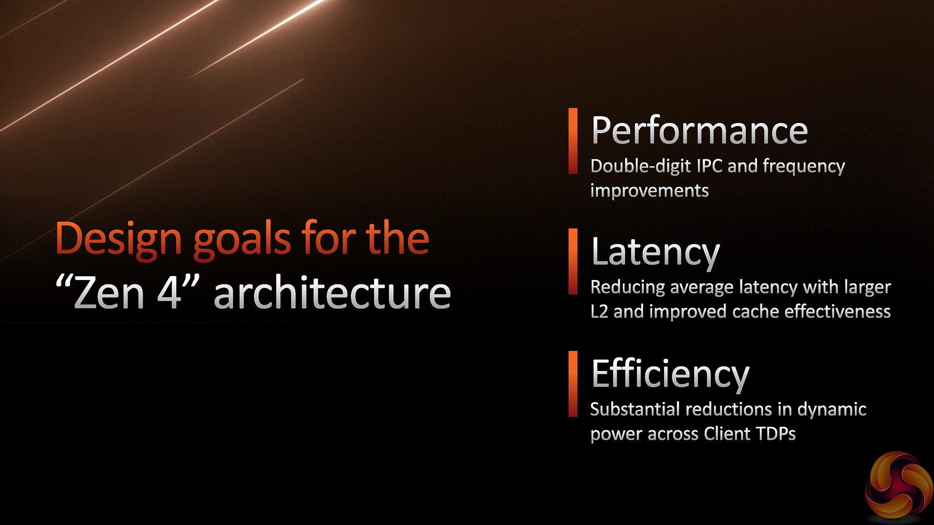
According to AMD, the key design goals for the Zen 4 architecture focused on efficiency gains, latency improvements, and better performance in terms of frequency and IPC.
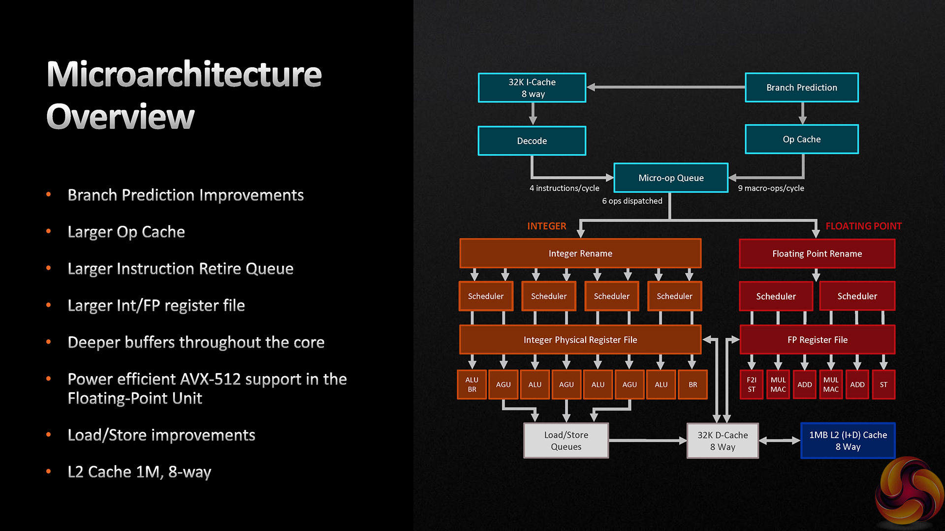
Changes to the cache structure allow AMD to enhance the data flow and reduce latency. One key area to this point is the doubling of L2 cache capacity to 1MB per core instead of 0.5MB per core on Zen 3.
Front-end, execution engine, and load/store advances are achieved via various measures. The enhancements are designed to improve the data flow for the new Zen 4 core versus Zen 3. And that’s particularly useful for better utilising the downstream resources whilst also reducing latency in the underlying architecture, particularly with that larger slice of L2 cache.
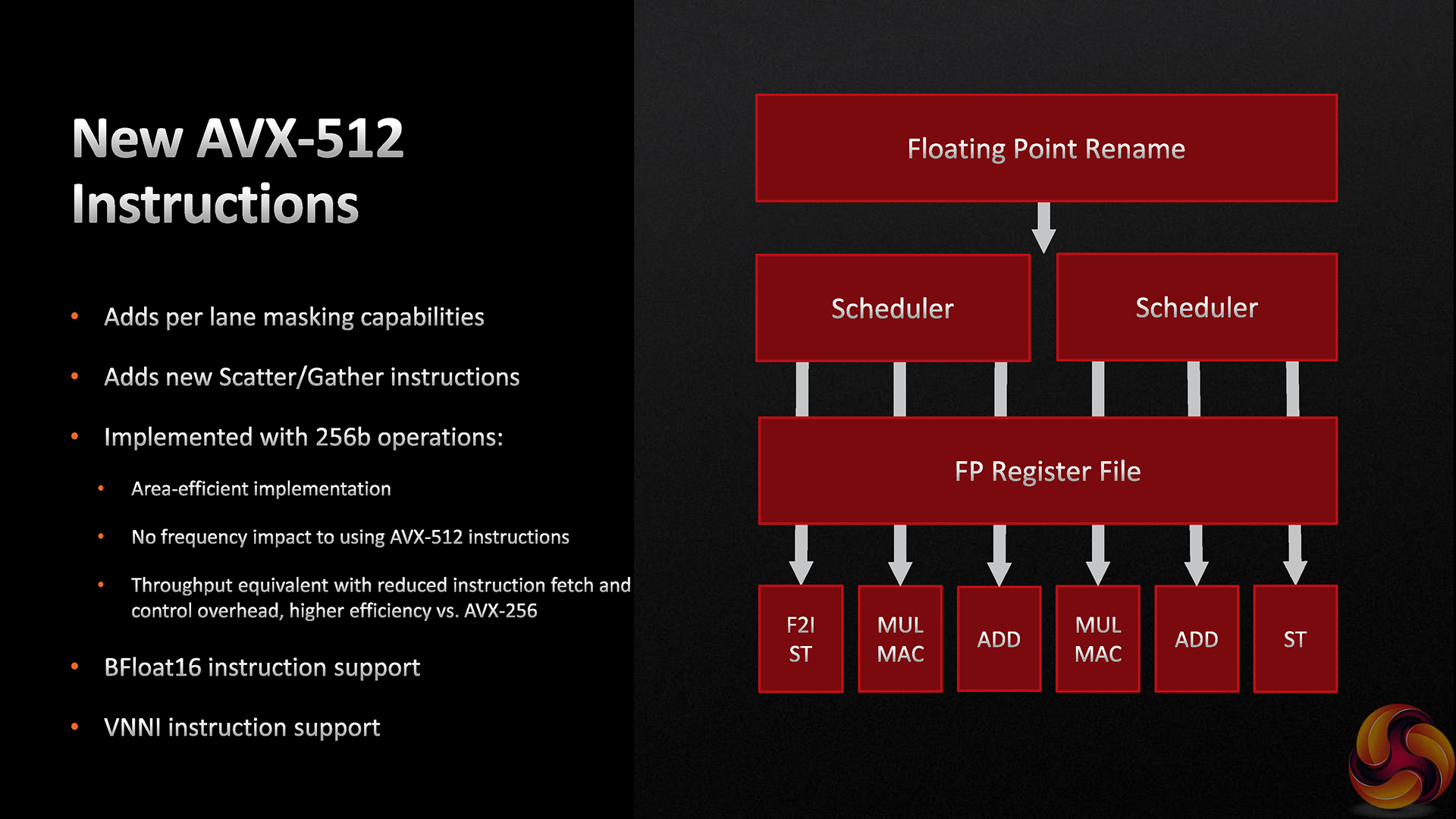
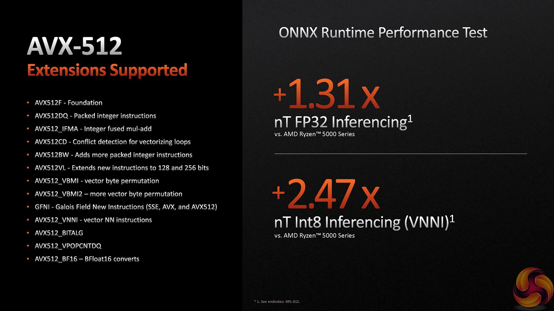
Another noteworthy enhancement to Zen 4 is AVX-512 support. This is technically handled via a double-pumping of the 256-bit wide data path, rather than a single operation, because AMD didn’t want to spend the core area of a full 512-bit data path.
While AVX-512 support is a cool inclusion, we have seen from Intel’s adjustments that it isn’t really a significant benefit for the consumer market currently. Zen 4 servers on the other hand – they’ll like that alongside BFloat16.
Ryzen 7000 CPU Configuration
The Ryzen 7000 chips use 8-core CCXs built on the TSMC 5nm process node.
The individual Core Complexes feature a 32MB slice of L3 cache – as we saw with Zen 3 – but no 3D V-Cache like we saw with the 5800X3D. We’ll have to wait for the V-Cache chips because AMD said they didn’t want to delay these parts.
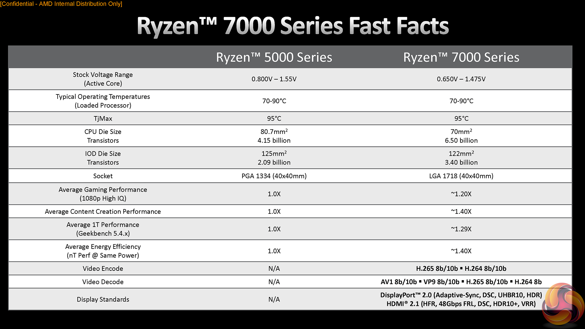
Each 8-core core chiplet measures in at 70mm2 with 6.50 billion transistors. That’s an area reduction versus the 80.7mm2 Zen 3 core chiplet which featured 4.15 billion transistors. Clearly, the density uptick of TSMC 5nm is substantial.
Aside from density, frequency is another huge improvement from 5nm. We now see boost clocks as high as 5.7GHz on the 16 core chip!
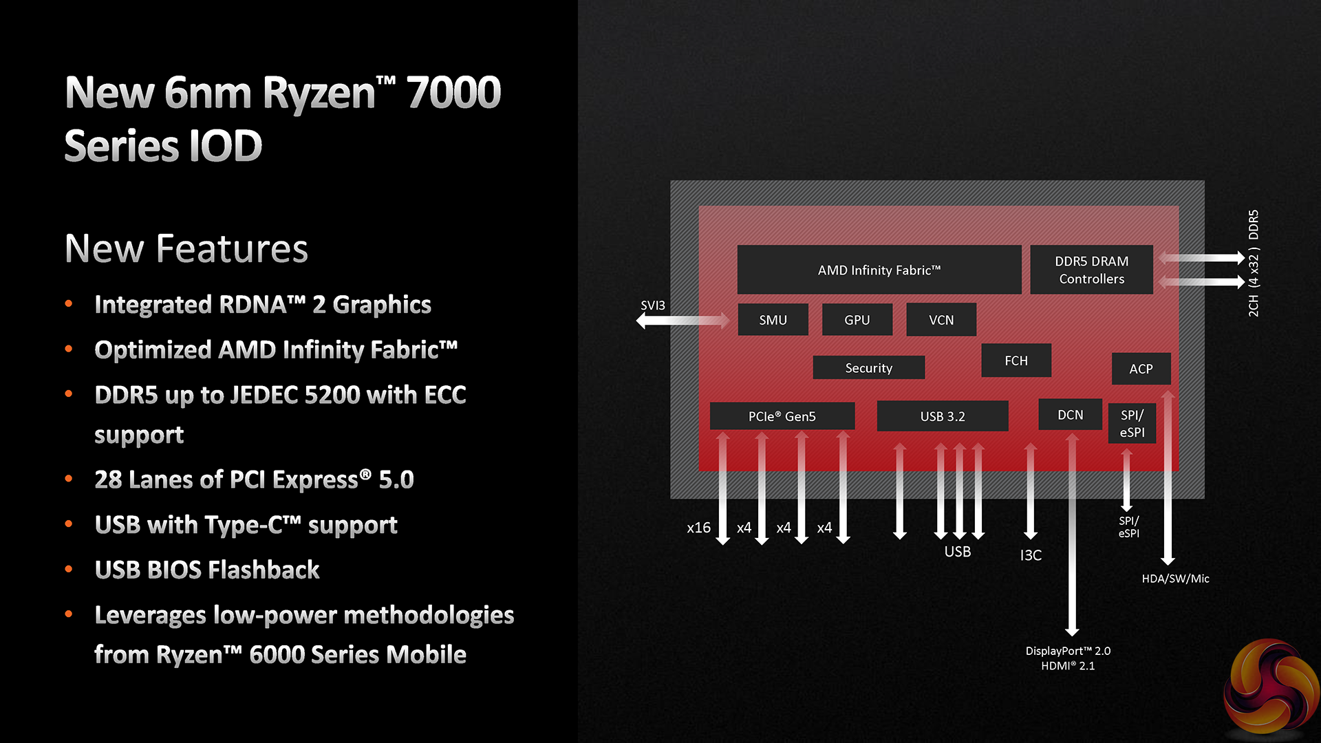
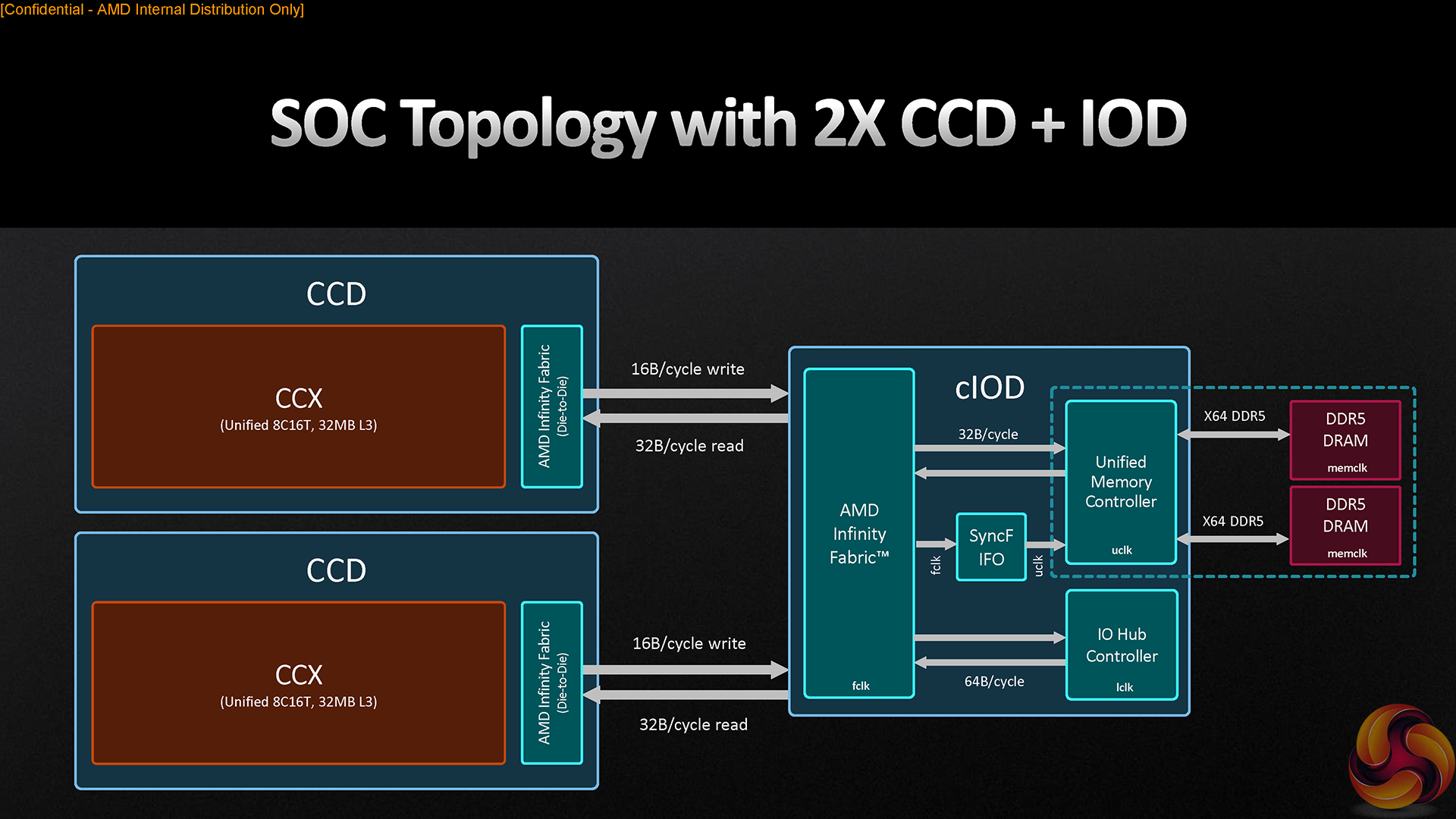
The new Ryzen 7000 Series IO Die is a substantial improvement versus Ryzen 5000.
Fabbed on the TSMC 6nm process node, AMD has gone for a more advanced, more expensive manufacturing option with its Ryzen 7000 IO Die. That’s actually a change of direction versus Ryzen 5000 that was built using significantly older 12nm process technology.
This decision allows AMD to increase the transistor count from 2.09 Billion previously to 3.40 Billion now, alongside a small decrease in die area from 125mm2 on Ryzen 5000 to 122mm2 now. And they jam a bunch more functionality onto the new IO chiplet, too.
We get 28 lanes of PCIe Gen 5, a dual-channel DDR5 memory controller that supports up to JEDEC-5200 and ECC, USB 3.2 and Type-C support, and USB BIOS Flashback.
AMD also includes low-power methodologies borrowed from the Ryzen 6000 Series Mobile processors, such as SOC power states, clock gating, and power gating.
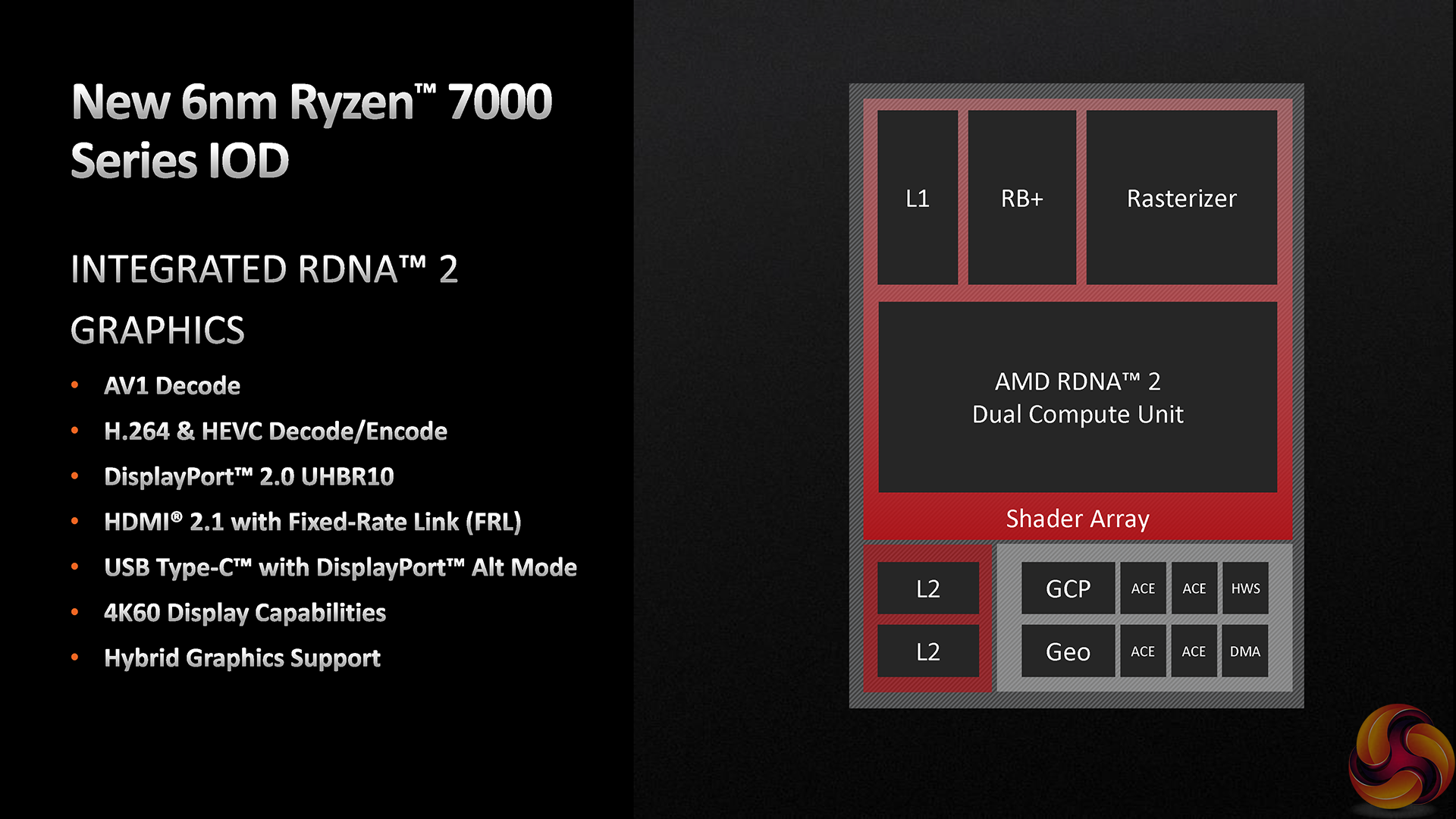
Importantly, the IO Die also features the integrated GPU that features two RDNA 2 Compute Units.
When we asked AMD about this inclusion during their tech day in Austin, Texas, the response was quite clear in that this was included to allow them to sell partner systems to businesses who require iGPU capabilities for powering a basic monitor.
As we have seen on the Intel side, though, the inclusion of a modern iGPU also has the benefit of allowing for competent media encode and decode capability