

Ampere brings with it several key changes in terms of the GPU architecture. Here we go over what you need to know.
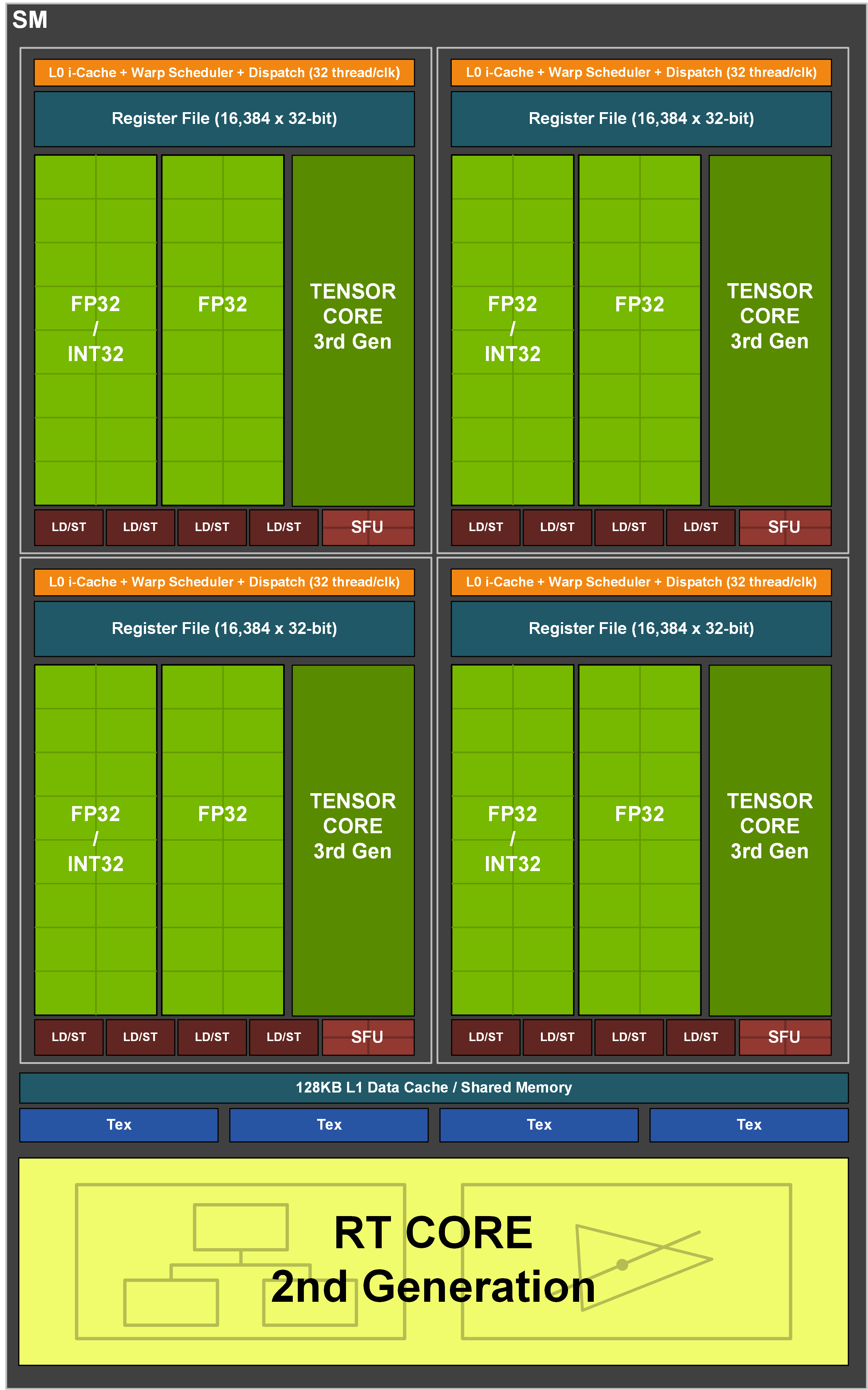
The New SM
Click to enlarge.
One of the headline-grabbing features of the RTX 30-series has been the ludicrously high core counts. Considering the RTX 2080 Ti launched with 4352 CUDA Cores, and that was the most populous of the 20-series GeForce stack, it was pretty astonishing to see even the RTX 3070 exceed that, while the RTX 3080 has double the cores.
This is a result of Nvidia doubling the number of FP32 ALUs per SM. Where Turing had a dedicated data path for INT operations, with Ampere this is now split between INT and FP32. Tony Tamasi, VP of Technical Marketing at Nvidia, explained this change as part of a Q&A on reddit:
“One of the key design goals for the Ampere 30-series SM was to achieve twice the throughput for FP32 operations compared to the Turing SM. To accomplish this goal, the Ampere SM includes new datapath designs for FP32 and INT32 operations. One datapath in each partition consists of 16 FP32 CUDA Cores capable of executing 16 FP32 operations per clock. Another datapath consists of both 16 FP32 CUDA Cores and 16 INT32 Cores. As a result of this new design, each Ampere SM partition is capable of executing either 32 FP32 operations per clock, or 16 FP32 and 16 INT32 operations per clock. All four SM partitions combined can execute 128 FP32 operations per clock, which is double the FP32 rate of the Turing SM, or 64 FP32 and 64 INT32 operations per clock.
Doubling the processing speed for FP32 improves performance for a number of common graphics and compute operations and algorithms. Modern shader workloads typically have a mixture of FP32 arithmetic instructions such as FFMA, floating point additions (FADD), or floating point multiplications (FMUL), combined with simpler instructions such as integer adds for addressing and fetching data, floating point compare, or min/max for processing results, etc. Performance gains will vary at the shader and application level depending on the mix of instructions. Ray tracing denoising shaders are good examples that might benefit greatly from doubling FP32 throughput.
Doubling math throughput required doubling the data paths supporting it, which is why the Ampere SM also doubled the shared memory and L1 cache performance for the SM. (128 bytes/clock per Ampere SM versus 64 bytes/clock in Turing). Total L1 bandwidth for GeForce RTX 3080 is 219 GB/sec versus 116 GB/sec for GeForce RTX 2080 Super.
Like prior NVIDIA GPUs, Ampere is composed of Graphics Processing Clusters (GPCs), Texture Processing Clusters (TPCs), Streaming Multiprocessors (SMs), Raster Operators (ROPS), and memory controllers.
The GPC is the dominant high-level hardware block with all of the key graphics processing units residing inside the GPC. Each GPC includes a dedicated Raster Engine, and now also includes two ROP partitions (each partition containing eight ROP units), which is a new feature for NVIDIA Ampere Architecture GA10x GPUs. More details on the NVIDIA Ampere architecture can be found in NVIDIA’s Ampere Architecture White Paper, which will be published in the coming days.”
GDDR6X Memory
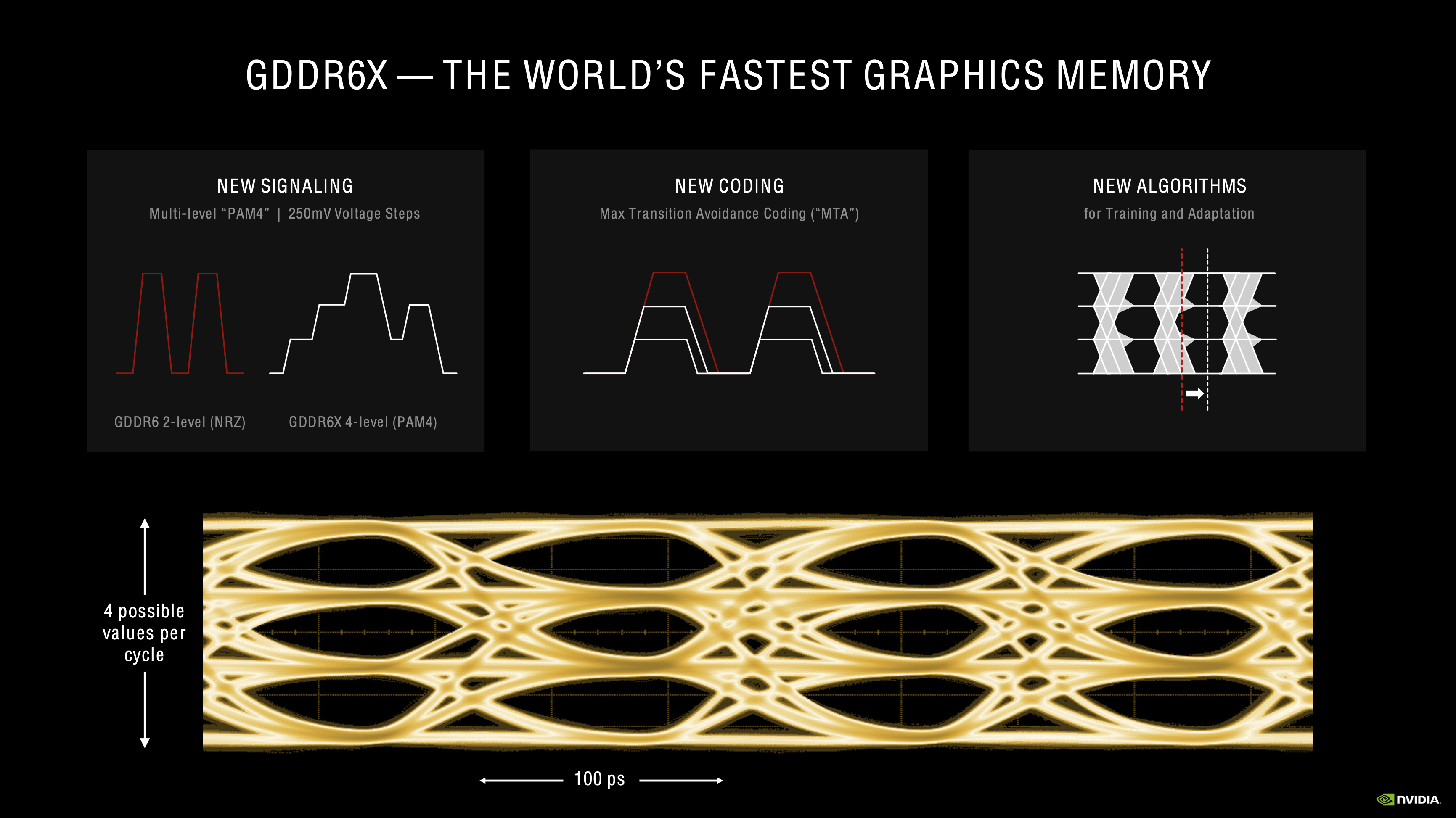
Another step forward is the use of GDDR6X memory with the RTX 3080 and RTX 3090, though the RTX 3070 will remain on GDDR6. Developed in collaboration with Micron, GDDR6X uses new 4-level Pulse Amplitude Modulation (PAM4) signalling instead of the previous 2-level NRZ signalling that is used with GDDR6 (non-X). Where NRZ signalling can only send binary data, PAM4 – as the name suggests – can send one of our voltage levels, in steps of 250 mV, per clock cycle. Nvidia claims this allows GDDR6X to ‘transmit twice as much data as GDDR6' memory.
RTX 3080 sports 10GB of GDDR6X, clocked at 19Gbps. Coupled with the 320-bit memory interface, memory bandwidth is up to 760 GB/s, while the RTX 3090 is capable of hitting bandwidth speeds of 936 GB/s.
Additionally, Nvidia has changed how the memory responds to overclocking – as we will see later in the review. Based on my experience overclocking the RTX 3080, I got in touch with Nvidia about this as they responded with the following:
“One of the design features we added to enhance memory reliability is transaction error detection and replay. That is, when the encoding shows that there has been a data transmission error, the transmission in error is re-tried or “replayed” until a correct memory transaction is successful. As you push overclocks and cause more errors, the re-tried transactions reduce useful memory bandwidth and thus reduces performance.
This feature actually increases memory frequency capability and pushes out the artifacts, crashes, and other negative impacts of overclocking to higher frequencies. Crashes can still happen if frequencies are pushed too hard. So, if performance starts dropping, you've actually passed the limit at which the system would have crashed. Rather than rebooting as feedback, plateauing performance indicates you’ve hit the limits of OC.”
RT and Tensor Improvements
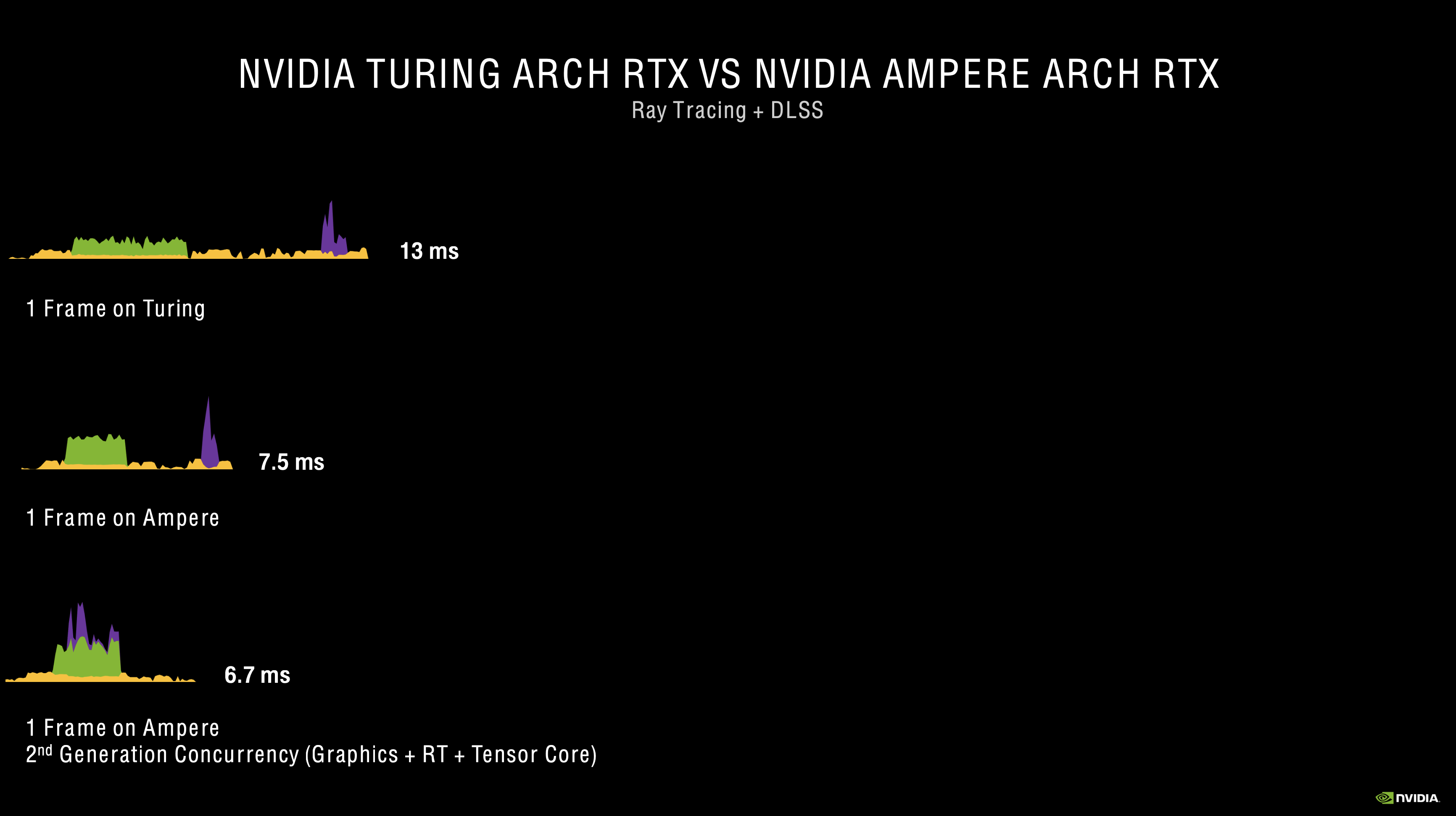
Alongside improvements to the Tensor Cores and RT cores themselves, Nvidia has also introduced what it calls Second Generation Concurrency. With Turing, the GPU was limited to executing the shader and RT pipelines concurrently, while any DLSS (Tensor) workloads had to come further down the pipeline. With Ampere, it is now possible to execute shader, RT and DLSS operations concurrently, improving performance to the end user.
Using Wolfenstein Youngblood as an example, if Ampere tried to render a ray traced frame through software, without using the RT or Tensor cores, Nvidia claims we would be looking at a frame time of 37ms, or about 27fps. Thanks to the RT cores, ray tracing is significantly easier to run than through software, so the frametime can be reduced to 11ms. Once DLSS is added to the workload via the Tensor core, the render time is further reduced to a 7.5ms frametime. Nvidia claims that executing all three operations concurrently, however, will improve performance further, with a frametime of 6.7ms, or 149fps.
RTX IO
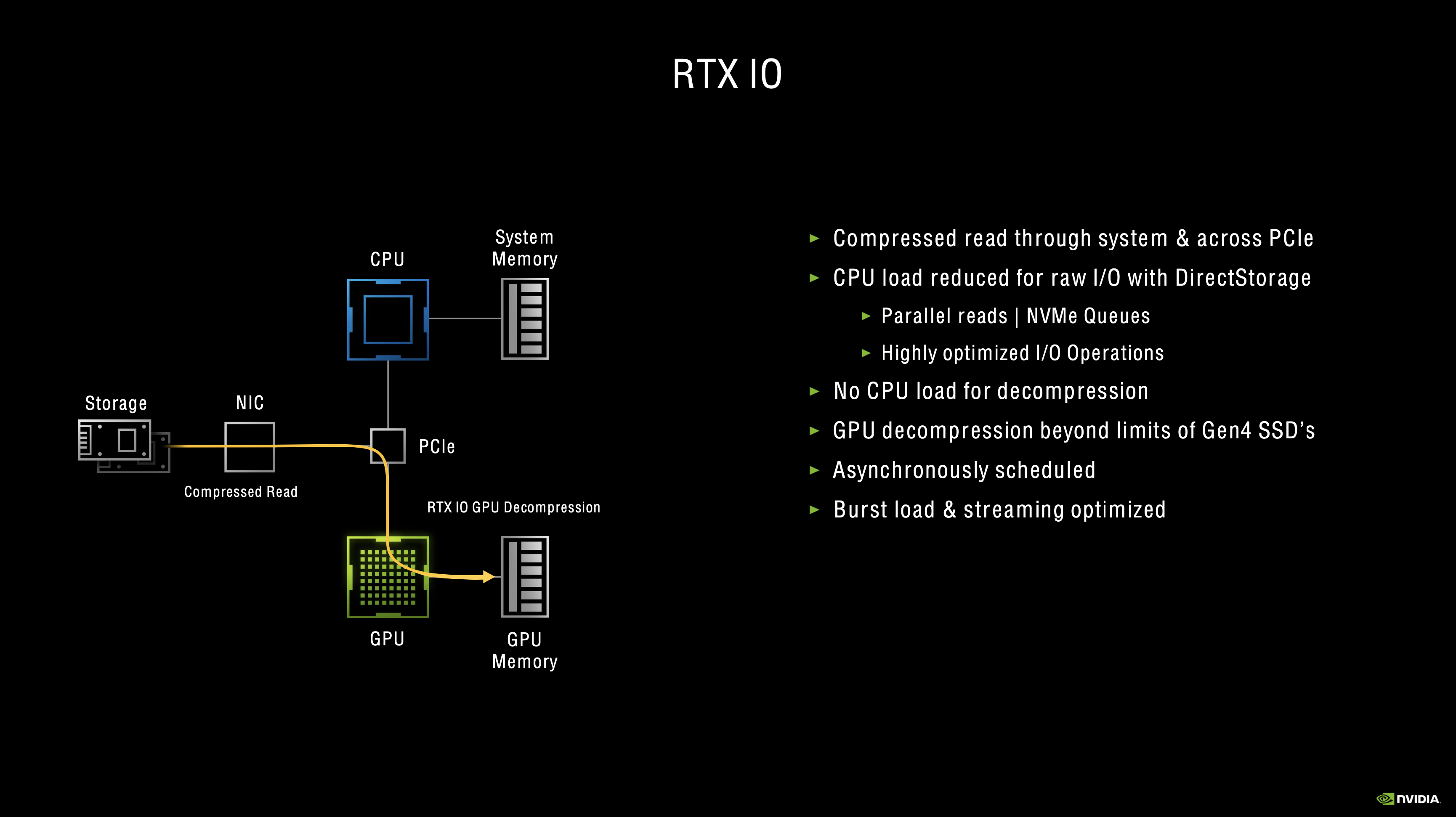
The last key feature we want to touch on here is RTX IO. Nvidia explains this by pointing to the ever-increasing speeds of SSDs, which are now wildly faster than traditional HDDs. The increased speeds, however, run into bottlenecks with the traditional I/O subsystems, which is why developers have been turning to lossless compression techniques. Nvidia claims that such techniques performed with a PCIe Gen4 SSD can utilise ‘tens of CPU cores', limiting I/O performance and impacting ‘next-generation streaming systems that large, open-world games need.'
The solution is RTX IO. This is a new API that aims to deliver GPU-based lossless decompression, moving work from the CPU and to the GPU which, Nvidia claims, can provide ‘enough decompression horsepower to support even multiple Gen4 SSDs. This can enable I/O rates more than 100 times that of traditional hard drives, and reduce CPU utilisation by 20x.'
The kicker is that RTX IO does need specific integration into games by the developers, so we can't just take an RTX card and speed things up in any old game. However, Nvidia says it is working with Microsoft to ensure RTX IO is cooperative with DirectStorage, as by using DirectStorage, ‘next-gen games will be able to take full advantage of their RTX IO enabled hardware to accelerate load times and deliver larger open worlds, all while reducing CPU load.'