

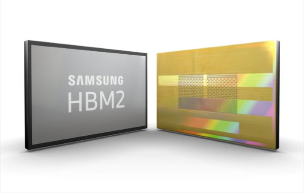
Samsung recently announced that they have developed the worlds first 12-layer 3D-TSV (Through Silicon Via) technology DRAM modules with up to 24GB capacity, one of the first products to use the technology will be Samsung’s very own HBM2 KGSDs.
Samsung’s new 12-layer 3D-TSV process features 12 DRAM chips interconnected through 60,000 TSV holes which is why this technology is considered as one of the most challenging packages for mass production, as it requires pinpoint accuracy. The thickness of the package remains at 720 micron which means DRAM layers are getting thinner, while still producing acceptable yields for high-end products.
“Packaging technology that secures all of the intricacies of ultra-performance memory is becoming tremendously important, with the wide variety of new-age applications, such as artificial intelligence (AI) and High Power Computing (HPC),” said Hong-Joo Baek, executive vice president of TSP (Test & System Package) at Samsung Electronics.
By increasing the number of layers from eight to twelve, Samsung will soon be able to offer mass production of 24 GB High Bandwidth Memory which will provide three times the capacity of current 8 GB high bandwidth memory available today. Meaning Samsung will produce the highest DRAM performance for data-intensive applications on the market.
In addition, Samsung’s latest 3D packaging technology features shorter data transmission times between chips than the current wire bonding technology, which will result in significantly faster speed and lower power consumption, increasing efficiency.
KitGuru says: This latest technological advancement from Samsung means we should see High-end graphics cards and FPGAs benefit from Higher memory bandwidth and capacities in the near future.