

Samsung Electronics indicated that it plans to start volume production of high-bandwidth memory (HBM) next year at the Intel Developer Forum this week. At the trade-show, the company revealed its current vision and expectations concerning HBM. Samsung foresees that eventually high-performance applications (such as GPUs) could feature up to six HBM devices to enable unprecedented capacities and bandwidth.
As it appears, Samsung plans to skip the first-generation HBM memory and will only manufacture products compliant with the second-generation HBM specification, which offers higher densities and clock-rates. Such approach will let Samsung to address broader market segments with its HBM offerings. Right now HBM can only be used on consumer graphics cards and certain highly-custom products, but HBM2 will enable professional and high-performance computing GPU-based solutions, which require a lot of memory onboard.
Samsung is currently working on multiple HBM packages featuring two (2Hi stack), four (4Hi) and eight (8Hi) 8Gb memory devices on a base logic die with 1024-bit interface, according to a slide that the company demonstrated at the IDF (which was published by ComputerBase.de). Maximum data-rates of Samsung’s HBM products will be 2Gb/s, which will support up to 256GB/s of bandwidth per chip.
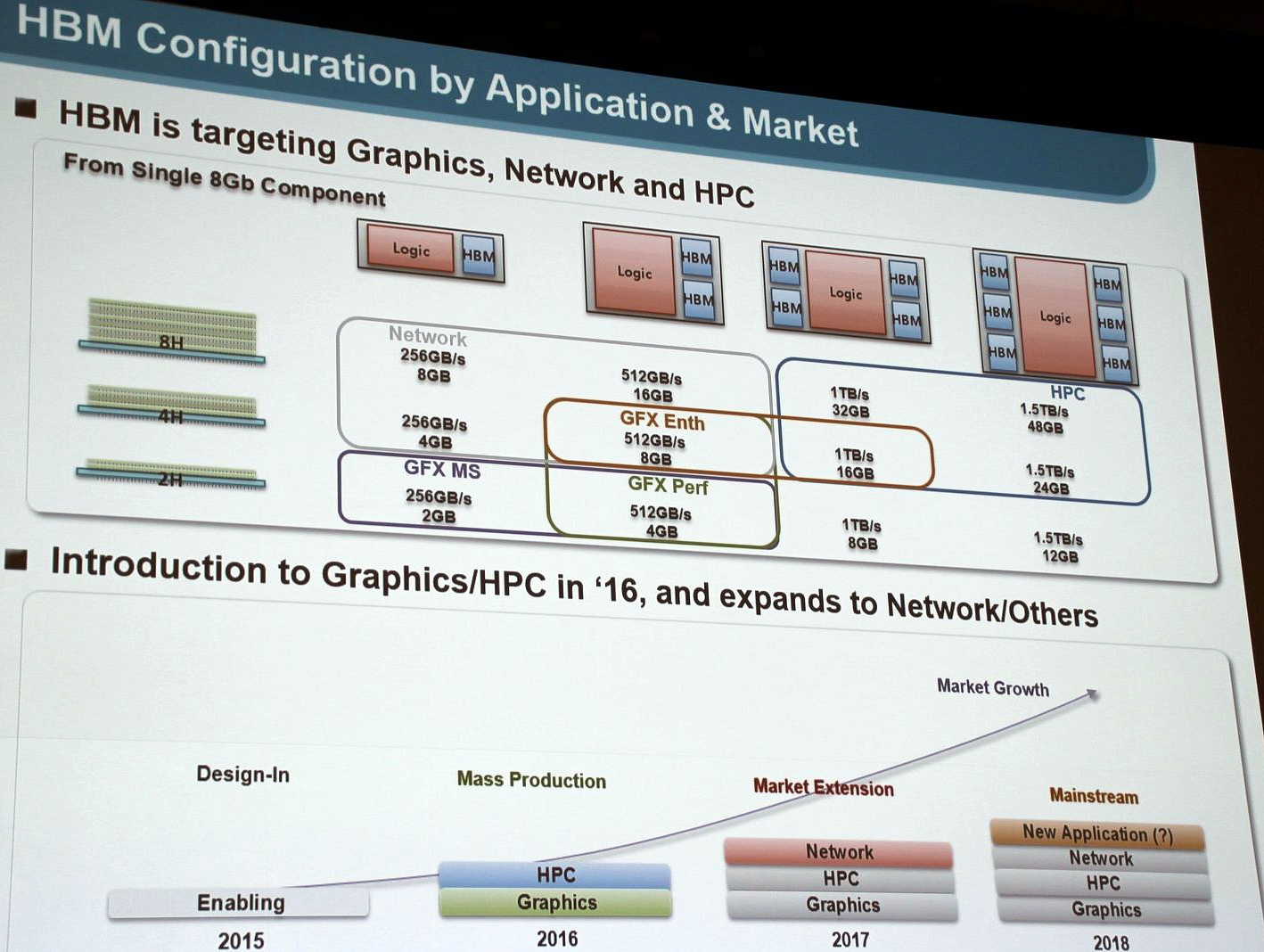
Samsung believes that HBM memory will enable it to create a variety of chip offerings targeting different market segments. Designers of logic chips (GPUs, APUs, network processors, etc.) will be able to integrate the right amount of HBM controllers into their chips in order to target different applications. At present AMD’s “Fiji” graphics processing unit supports up to four HBM stacks over its 4096-bit interface. Eventually, logic chips could accommodate more HBM controllers and expand interface width to unprecedented 6144-bit, according to Samsung Electronics.
For example, a mainstream graphics card could use just one 2Hi HBM chip to accommodate a 2GB frame-buffer with 256GB/s bandwidth. More advanced graphics adapters for consumers and creative professionals could feature four 2Hi or four 4Hi HBM stacks that provide up to 1TB/s of bandwidth as well as 8GB, 16GB or 32GB of memory. Accelerators for high-performance computing as well as ultra-high-end GPU offerings will support six HBM stacks, thus enabling cards with 12GB, 24GB or 48GB of onboard memory with 1.5TB/s bandwidth.
So far, neither AMD nor Nvidia have demonstrated even hypothetical product implementations (which are used to showcase potential future uses of technologies) of GPU-based solutions featuring six HBM memory chips. Intel Corp.’s Xeon Phi co-processors use HMC [hybrid memory cube] DRAMs as “near memory” and are not expected to support HBM any time soon.
Samsung expects HBM memory to be used for consumer graphics cards and high-performance computing accelerators based on AMD “Arctic Islands” and Nvidia “Pascal” graphics processors next year. Sometimes in 2017, network products will also take advantage of the new memory type. Three years from now other applications could employ HBM, according to Samsung.
The world’s largest maker of dynamic random access memory (DRAM) did not unveil any details about its actual HBM chips (capacities, clock-rates, etc.), but expect a family of products with different densities and frequencies.
Samsung did not disclose which process technology it will use to manufacture HBM.
Discuss on our Facebook page, HERE.
KitGuru Says: Samsung is definitely not the first to offer HBM, but it is pretty clear that the company takes the new type of memory very seriously. What is interesting is that the company decided not to give a glimpse into the future of HBM, which indicates that the third-generation HBM is still a work in progress.

I’m excited for what Samsung is gonna do here, they always seem to rise at the top of any industry they take on and bring innovation.
That’s not innovation. HBM 2 is already in the works by Hynix. Samsung will be just another manufacturer of it
Intel Xeon Phi uses MCDRAM which is not Micron’s HMC. MCDRAM uses the same fundamental technology as HMC, but is a custom device for Phi. As for HBM innovation?? HBM has been under standards definition in JEDEC for years. It’s hard to say there is any one innovator.
Samsung is building the highest performing chips at the lowest voltage. I’d say that’s innovation.
Not talking about this in particular, but in general. For instance they got in the SSD market and now they’re dominating it with their innovative 850 EVO with 3D V-NAND.
to bad their monitors and tv suck hard
❖❖❖❖❖❖❖❖❖❖❖❖❖❖❖❖❖❖❖❖❖❖❖❖❖❖❖❖❖❖❖❖❖❖❖❖❖❖❖❖❖❖❖ my right hand’s stride sister makes 94$ dependably on the tablet……..on Sat I got a prime of the degree audi sinceobtaining a check for four216$ this most divide 4 weeks moreover, i truly started six months/previous and on an especially clear level in a brief moment was making more than 87$ p/h . try this site………….
✔✔✔OVER HERE✔✔✔ tinyurl.com/Jobs8zReportOnlinega1 __________________________________________________________________________ ➽➽➽➽➽➽➽➽➽➽➽➽➽➽➽➽➽➽➽➽➽➽➽➽➽➽➽➽➽➽➽➽GO TO THIS AND CLICK NEXT LINK IN IT FOR WORK ✔✔✔✔✔✔
Hynix also does HBM 2 memory and at the moment there no info about who offers fastest HBM 2 and that doesn’t have any relevance either. Yes I can read your psychi that you wanted to diminish the value of Hynix-AMD HBM partnership. Poor soul.
but now they lost war intel/miron win
Any company that has access to Hynix and AMD’s HBM2 can do that lol, that’s not innovation, sorry.
Can’t vouch for those but certainly get annoyed when washing machine finishes and plays a stupid chime/song! Had to google search how to turn that crap off real fast. lol
They don’t have access to Hynix’s chips. All Samsung is doing is building chips to the HBM 2 standard as highlighted in the JEDEC whitepapers (anyone in JEDEC can make chips according to that standard), but they are building chips with 50% higher capacity, 50% higher bandwidth, and 10% lower power and heat. Sorry, but that’s innovation by definition: change what exists to make it more perfect.
You’re likely thinking of the definition of invention and confusing the terms.
We know what Hynix’s specs are. They were here on wccf not more than 2 months ago. 8GB maximum capacity per 8-hi stack with 250GB/s bandwidth per stack, a 4-stack configuration resulting in 1 TB/s bandwidth. Samsung is now offering 12GB per 8-hi stack at 375GB/s per stack to reach the reported 1.5TB/s bandwidth for a 4-stack configuration.
Its occurred to me that the South Koreans are like the Japanese in that respect. Adding humanity to things. They do it better though, as they want it to be endearing but not perverted.
“The world’s largest maker of dynamic random access memory (DRAM) did not unveil any details about its actual HBM chips (capacities, clock-rates, etc.), but expect a family of products with different densities and frequencies.”
18 billion trannies will need every GB
drashek
Doesn’t matter. AMD and Nvidia have already announced their cards will be 32GB at the most. Samsung is now offering a 48GB configuration in 4 chips. Therefore we know the specs of both. Seriously, is inductive and deductive reasoning this difficult for you people? Have any of you graduated high school?
“Samsung is now offering a 48GB configuration in 4 chips.”
“The world’s largest maker of dynamic random access memory (DRAM) did not unveil any details about its actual HBM chips (capacities, clock-rates, etc.), but expect a family of products with different densities and frequencies.”….
kinda saw it comming
I’d wish that my dishwasher would learn from the Japanese and South Koreans. Whenever I complain about it being so slow, it tells me to “fuck off”.
….I should get another girlfriend.
*ba dum tcsh!*
then use gpu vram as system ram. No need for ram lol.
48GB configuration in 6 chips, not 4 chips. Take a look at the slide.
8GB per 8-hi stack, not 12GB per 8-hi stack. Stop making up and inflating numbers.
That’s a big problem when a company pretends to be good in everything.
That’s what APUs are doing and will probably do with HBM.
No, Samsung found a better solution to fit more per stack.
it’s 48 in 4, and I did see the slides.
I am asking you where do you get those numbers?
Samsung’s own presentation on the matter a few months back. The slides should still be up somewhere. It was shortly after the Hynix announcement about priority access for AMD.
You still don’t give a concrete answer, stop dodging the question.