

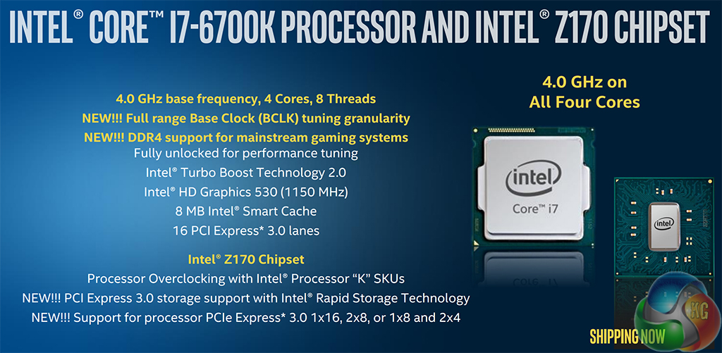
While the slide specifically references the Core i7-6700K, many of its points are true for the Z170 platform as a whole.
One of the key differentiators when it comes to overclocking is that Intel has decoupled the CPU BCLK and the PCIe clock for Skylake. With Sandy Bridge's 2011 introduction, Intel effectively locked down the BCLK and prevented its overclocking capacity. This gave users a very limited freedom (typical less than 8%) to adjust the BCLK, forcing reliance upon the CPU core ratios for overclocking. Intel has been a little more open about BCLK adjustments in recent generations – the 100MHz, 125MHz, 167MHz BCLK straps for Haswell and Ivy Bridge-E were useful.
Skylake's clock decoupling allows full adjustment of the CPU BCLK without having a negative effect on other system components. There's a full range of capabilities with 1MHz increments, which means that good ‘ol fashioned BCLK overclocking is well-and-truly back. Some of the older overclockers accustomed to Intel's pre-Sandy Bridge platforms will be glad to see the return.
And to those who have delved into the scene of overclocking since the release of Sandy Bridge, the straightforward core ratio overclocking procedure still exists thanks to an unlocked multiplier for K series SKUs.
The Core i7-6700K uses Intel's HD 530 on-chip GPU. We do not actually have much information relating to the GPU, although we know that it is clocked at 1150MHz and is likely to be faster (and consume more power) than Devil's Canyon's iGPU. We aren't going to focus on iGPU performance today as the vast majority of gamers and enthusiasts will be opting for a dedicated graphics card.
Another of the key differences when it comes to CPU operation is that Intel has pulled the on-chip voltage regulator (known as the Fully-Integrated Voltage Regulator, or FIVR for short) out of the CPU and handed this control back to motherboard manufacturers. This removes the requirement for a separate input voltage that drives the FIVR and therefore simplifies overclocking by removing one of the voltage settings.
Unlike the HEDT chips, Intel's mainstream CPUs, Skylake included, utilise Thermal Interface Material (TIM) rather than solder to bond the CPU die and heatspreader. This manufacturing method reared its ugly head with the initial Haswell CPUs which suffered from high operating temperatures due to the limited heat transfer capacity of the TIM and heatspreader/die bond.
Intel fixed the Haswell problem by implementing its Next-Generation Polymer Thermal Interface Material (NGPTIM) on Devil's Canyon, which resulted in a temperature decrease of more than 10% in our testing. That still doesn't deviate from the point that any form of polymer TIM is, almost certainly, less thermally conductive and effective than the solder that HEDT chips use.
With that said, we would hope that the shrink to 14nm transistors and lessons learned with Devil's Canyon will help Skylake to manage its thermal performance better than initial Haswell processors did.
Skylake CPUs fit into Intel's newly-released LGA 1151 socket. Yes, that is a single extra pin over the LGA 1150 socket that it replaces. Consumers show frustration regarding Intel's short-lived CPU socket progression, so the company addressed this point at the Skylake press seminar.
The new socket forces users to invest in the accompanying motherboard (which will feature the latest chipset and its partnering features) if they want to upgrade their CPU, rather than just drop the new chip into an older motherboard. Everybody will have an opinion on this mindset, however Intel pointed out that their engineers and architects design the platform as a whole rather than segregate the CPU and motherboard (socket and chipset). That point is more understandable from a technological advancement perspective – it may be just one pin on the face of the situation, but there are significant under-the-hood changes to the CPU and platform.
Using a legacy motherboard with its older power delivery design and PCB traces could potentially make it impossible for some of the platform changes to be implemented. I highly doubt that Skylake's significant power delivery change, for example, would have been possible if reapplication of LGA 1150 motherboards designed for Haswell's FIVR was made a design criteria.
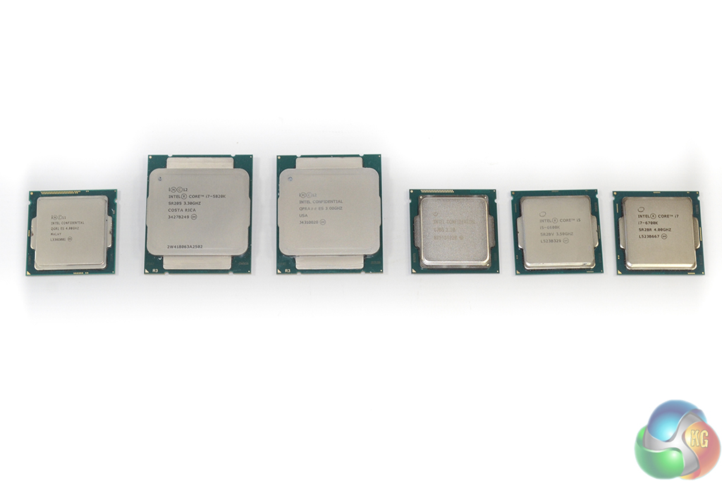
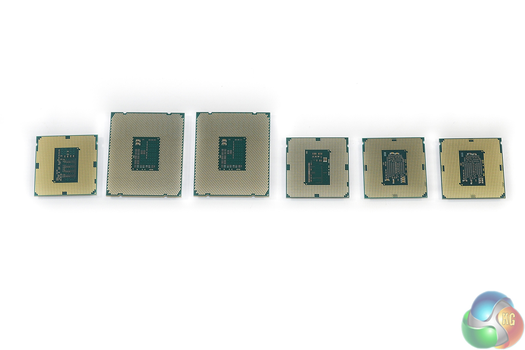
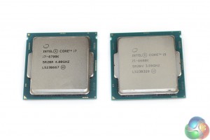
From left to right: Devils' Canyon i7-4790K, Haswell-E i7-5820K, Haswell-E i7-5960X, Broadwell i7-5775C, Skylake i5-6600K, Skylake i7-6700K.
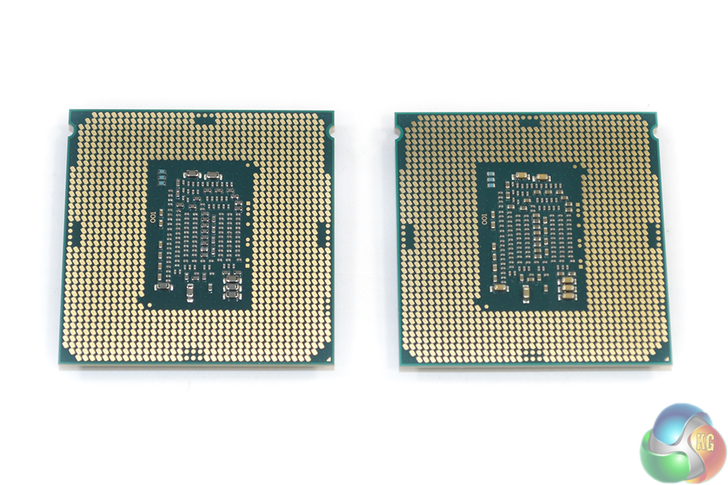
Skylake's CPU sizing is practically identical to previous mainstream processors. That's important because it means that mITX motherboard designs are actually possible and can be recycled for the Z170 platform. The physically large Haswell-E CPUs present a significant challenge for motherboard vendors attempting to make a mITX X99 motherboard.
The only other significant physical differences between the LGA 1150 and LGA 1151 CPUs are a change to notch positioning and a significantly more dense power delivery system for Skylake chips.
There's also the cluster of extra pins (overlapping the area of pin absence on each side of the CPU) that could be used to unlock additional settings as we have seen with Asus' OC Socket design for LGA 2011-3 CPUs. A recent news article pointed towards LGA 1151 OC Socket designs, which will indeed be incorporated on Asus' higher-end SKUs. The effectiveness of such a design depends on whether or not motherboard vendors can extract any useful benefits from the pins.
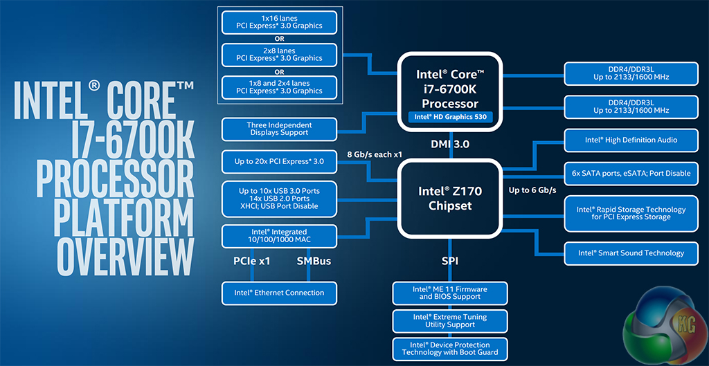
At the heart of the platform is the LGA 1151 Skylake CPU. Memory support is provided for DDR4-2133MHz and 1.35V DDR3L-1600MHz officially, however DDR4 speeds and DRAM divider support of up to 4133MHz have been claimed possible by Intel. This is the mainstream platform, so memory runs in dual-channel operation and most mATX and ATX motherboards will support up to four DIMM operation.
One of the most substantial upgrades comes from Intel's application of DMI 3.0. The latest version of the CPU-to-chipset Direct Media Interface uses PCIe 3.0 lanes which offer double the bandwidth of their PCIe 2.0 predecessors. Although Intel could not give us the official link speed, a look inside Asus' Z170 UEFI implies (we cannot certify it) that DMI 3.0 operates at a total bandwidth of 32Gbps via four 8GT/s lanes. If true, that translates into a 4GBps connection between the CPU and chipset, which is roughly enough speed to satisfy a pair of Intel SSD 750 PCIe drives in RAID 0. On that same point, the Z170 chipset and latest RST drivers support RAID for PCIe storage drives.
Running off the feature-healthy Z170 chipset are six SATA 6Gbps ports, up to 14 USB ports in total (up to ten of which can be USB 3.0), and up to twenty PCIe 3.0 lanes. Intel uses its flexible IO ports (FlexIO) to allow motherboard vendors to choose the combination of outputs that best suits their specific SKU. Intel told us that up to 26 of these flexible lanes are available, although the limitations as to the minimum number of a certain output were not disclosed. So, in theory, a configuration along the lines of six SATA 6Gbps connectors, four USB 3.0 ports, and 16 PCIe 3.0 lanes may be plausible. That opens up multi-GPU potential through the chipset's PCIe 3.0 lanes.
We asked Intel why USB 3.1 wasn't baked onto the chipset by default and the response was because they think that Thunderbolt 3 is the better solution. Obviously motherboard vendors disagree as the vast majority of their boards use add-on USB 3.1 chipsets from the likes of ASMedia, Intel, and EtronTech.
The Skylake CPUs support sixteen PCIe 3.0 lanes. That bank of sixteen can be deployed as 1×16, 2×8, or 1×8 + 2×4, making 2-card SLI (which demands a minimum x8 link) and 3-card CrossFire possible. That, if you ask me, is not a particularly future-proof decision on Intel's part. Users wanting 2-card SLI or high-bandwidth CrossFire in addition to a PCIe 3.0 x4 NVMe SSD (which are set to become far more commonplace over this platform's life-cycle), will be forced to handicap the ultra-fast storage drive by running it through the higher-latency chipset-fed PCIe 3.0 lanes. Outfitting the CPU with 20 PCIe 3.0 lanes would have been a smarter move.
Put simply, if you want to use two graphics cards with a PCIe 3.0 NVMe SSD, or more than two GPUs, the X99 platform and its plentiful PCIe connectivity is perhaps the best way to go.
The overall platform adjustments are, arguably, where Skylake shows its greatest improvements. While the platform may have its shortfalls, the chipset is a significant and welcomed improvement over yesteryear's Z97 offering. It is refreshing to see that Intel is finally equipping the chipset with PCIe 3.0 lanes, as this gives motherboard vendors extra flexibility to deploy add-on controllers (high-speed storage, USB 3.1, Thunderbolt, etc.) without siphoning off the CPU's limited number of lanes.

Like the review but leaves me wondering what’s point in upgrading
1.4 volts is too much .. 1.35 is at most what I would consider 24×7 safe with folding for years on end.
Great review, love the OC comparison to HW-E, the only site has done this so far.
If you’re folding 24/7, then you are probably right that 1.4V is a bit too much as it likely to hinder your CPU lifespan. But for most users who are not hammering the CPU 24/7, all of the signs in our testing and the discussions that we have had suggest that 1.4V is indeed fine.
Obviously we can’t certify that with just a handful of chips and a testing period spanning weeks not years. But temperature levels are typically a good indicator of what is safe and what isn’t.
Really there is no point to upgrade if you have a 4XXX i7, I hope AMD will get their shit together and release something really competitive because intel is dominating now and they doesn’t seem to care enough to push for better performance.
“With a very small pricing difference between an i7-6700K system and one based around the i7-5820K…”
From what I’ve seen so far the 5820k is going to cost you a hundred dollars more, so I guess there’s some difference of opinion on what constitutes a “small” pricing difference….
Well if you’re making a long term purchase (3yrs+) then a 5820 with 6 slightly slower cores will be a far better purchase than a 6700K, those two extra cores will start to pay dividends further down the line.
5820k £293 https://www.overclockers.co.uk/showproduct.php?prodid=CP-546-IN&groupid=701&catid=6&subcat=1672
6700k £299 https://www.overclockers.co.uk/showproduct.php?prodid=CP-582-IN&groupid=701&catid=6&subcat=3069
Yay, sub 10% X86 performance gains. And here we thought Skylake was going to have significant gains. Maybe Kaby Lake or Cannon lake with be significant over Haswell. But not holding my breath.
I don.t think people on buget like me should change from ivy brige (i5 3570k or i7 3770k) to this one …
Can you explain why?
zen cpu’s are going to be about 50 per cent faster per core than fx cpu’s so yeah intel will still have a pretty good speed advantage
6700k £263.99 – http://www.ebuyer.com/718338-intel-core-i7-6700k-4ghz-socket-1151-8mb-l3-cache-retail-boxed-processor-bx80662i76700k
5820k £306 – http://www.ebuyer.com/661535-intel-core-i7-5820k-3-30ghz-socket-2011v3-15mb-cache-retail-boxed-processor-bx80648i75820k
So about $100 for the americans, 40quid for us.
I’m now totally and utterly torn. I want to upgrade my i7 920 @ 4Ghz, but I just don’t have a clue to which. They are far too close, and with no real DX12 benches to go by, it’s difficult to say if those extra cores will come into play. There is every chance they will of course, but at this point, its too damn close.
Umm the AMD Zen chips are 40 percent in IPC over Excavator and without the Excavator IPC enhancements its on par with Haswell
Can’t wait for the i7 6820k !
not just the extra cores, but the extra cache and extra pcie lanes all add extra value and potential performance gains over these quad core chips. X99, like X79 and X58 before it, has much longer legs than Z170 and the lowest (I7-5820K) chip is within reach (~$50) of the I7-6700K.
of course they will come into play. during testing of the new OS they’ve already demonstrated significant improvement in multi core utilization/optimization. it’s only going to get better as software developers get working with it.
I totally hate the lack of older CPU’s (2600K or 3770K etc) in this review, but kudos for including oc’d Skylake results.
Single Threaded performance is still king. 6 cores won’t be mainstream for years.
You believe marketing more than you should.
lol@folding. people still do that?!
Its not marketing WFFCTech and RedGamingTech theorized it would be but it definitely isn’t going to be a slouch.
Roflmao!
What’s the incentive for “significant gains”? Without competition, there is no need. This isn’t about making us upgrade; they couldn’t care less if we postponed forever, all Intel cares about is that we choose them after our hiatus. If we go to another brand (whether it be AMD, or going the ARM route since most users aren’t gamers), then only would Intel up the bar to make any remaining stay loyal to them.
Haswell-E doesn’t have iGPU, you’re thinking of Haswell/Devil’s Canyon.
either way i expect you’re gonna be happy with a chipset upgrade 🙂
Yup. Though, the TDP and efficiency of the chips wouldn’t be lacking because of lack of competition would it? It’s because they are concentrating on iGPU performance I guess. Probably could squeeze more efficiency or computation/watt if they felt like it!
Me too. We specifically went out and bought a 2600K to act as a comparison because we didn’t have one at hand. But the time period given for testing the new hardware was really tight so we chose to include a full set of OC results on the chips we tested, rather data from older CPUs. This allows people to decide whether they want to wait for large scale availability to buy Skylake or whether Haswell-E (or a DC bargain, if they can get it) is better for them.
We’ll be including data from the older chips in the upcoming articles we have planned.
LMAO WCCFTECH?
Luke, if you get a chance, would you comment on the availability of HDMI 2.0 and HDCP 2.2 on these MB’s. It seems Gigabyte holds the most promise, but I haven’t been able to find any supporting documentation in that regard.
Oh, I hear it’s because of the serial nature of general purpose processors. They can’t make the integer/floating point units and more numerous per core, because the Instruction Scheduler couldn’t keep the pipeline full because of indirect and conditional branches. Maybe if the Scheduler could do some math itself and predict further..
1.4 volts to achieve 4.7GHz is an indication of really poor ASIC quality. I would wait for Skylake-E.
Why would a good cause go out of style?
Thing is, the single threaded performance is literally only a little better than Haswell.. Nearly all reviews show that, and some like OC3D say the Skylake chips are awesome while bashing the 5820k.. No sense at all.
Not true anymore. A vast majority of software and games use two or more threads now.
1.4V is fine for daily use on liquid cooled systems as temps are always kept in check. I’ve been running my 3930K @ 4.5Ghz @ 1.41V liquid cooled daily for almost 5 years and have had no issues whatsoever.
Don’t hold your breath. No miracles are going to arrive with Skylake-E. For noticeable improvements to TDPs and OC potential, look further in the future to Cannonlake and beyond.
…too bad they didn’t provide the idle and load temps for HW and HW-E…I noticed immediately how those figures were conveniently missing…lol What I can tell you is that I recently switched from a 4690K to a 6600K system build. Using the exact same cooler and TIM, the differences in temps at idle and under load are HUGE. 4690K @ idle = 36C 6600K @ idle = 21C. 4690K @ load (Prime95; Small TFTs bench) = 80C 6600K @ load (Prime95; Small TFTs bench) = 60C. The 6600K ran 20C cooler – that is no joke, and was reason enough for me to upgrade!
Thanks to further delays with 10nm FinFET the HEDT platform will now be two generations and a process node behind. I don’t even see the point of Skylake-E anymore if 4/6/8-core Cannonlake parts are going to be released in the same year.
“stock-clocked Skylake Core i7-6700K”. I don’t see stock cooler.
Is 1.42Vcore voltage, too high for a spiked voltage on the 6700K?
That’s awesome! Thanks for sharing that data. I’ll set up i7 6700K soon and update on my temps here.
What is folding?
or not cause by the time the 6 cores are really usefull vs , the higher clock frequency of a 6700 you’re 5820 will be crap anyway (and the 6700 too)
right but i upgraded anyway not for the small gains but i had a 3770k so now i can have m2 ssd as well as sli which i couldn’t before on my previous mb as well as many usb 3.1 ports etc etc
Cool
http://folding.stanford.edu/ It’s a project doing research into various diseases. Really cool thing. Not sure why Jimmy would be laughing at trying to cure things like cancer and Parkinson’s and Alzheimer’s. Even as of years ago tons of published research had already used Folding @ Home as part of their research.
yup, either buy 6600k or skip the 6700k to buy 6800k. Then it makes sense.
I run 4690k at 1.4v for months.
We apply very near maximum settings in Grand Theft Auto V and a 1920×1080 resolution to push today’s hardware. Our data was recorded using the built-in benchmark.