
The £210 price point is where we start to see X570 motherboards with an alluring set of features and capable power delivery solutions. But just how good are the power delivery systems on these ‘affordable' X570 offerings? We grab our Ryzen 9 3900X 12-core, apply a hefty overclock, and position a bunch of thermocouples to find out.
We have one competitor from each of the main four motherboard vendors' product stacks at the £210 price point.
For ASRock, we got a sample of the £210 X570 Steel Legend. ASUS sent across the TUF Gaming X570-Plus Wi-Fi, which is the same as the £210 non-Wi-Fi version for this test. We bought Gigabyte's £210 X570 Aorus Elite. And MSI's MPG X570 Gaming Edge WiFi was put on the credit card.
We are testing each of these motherboards with a heavy 4.25GHz, 1.35V overclock applied to our 12-core Ryzen 9 3900X. This represents a pretty demanding workload for these budget orientated X570 offerings. The X570 platform is expensive, so it'll be interesting to see if strong, capable power delivery systems are included in the bill with each of these offerings.
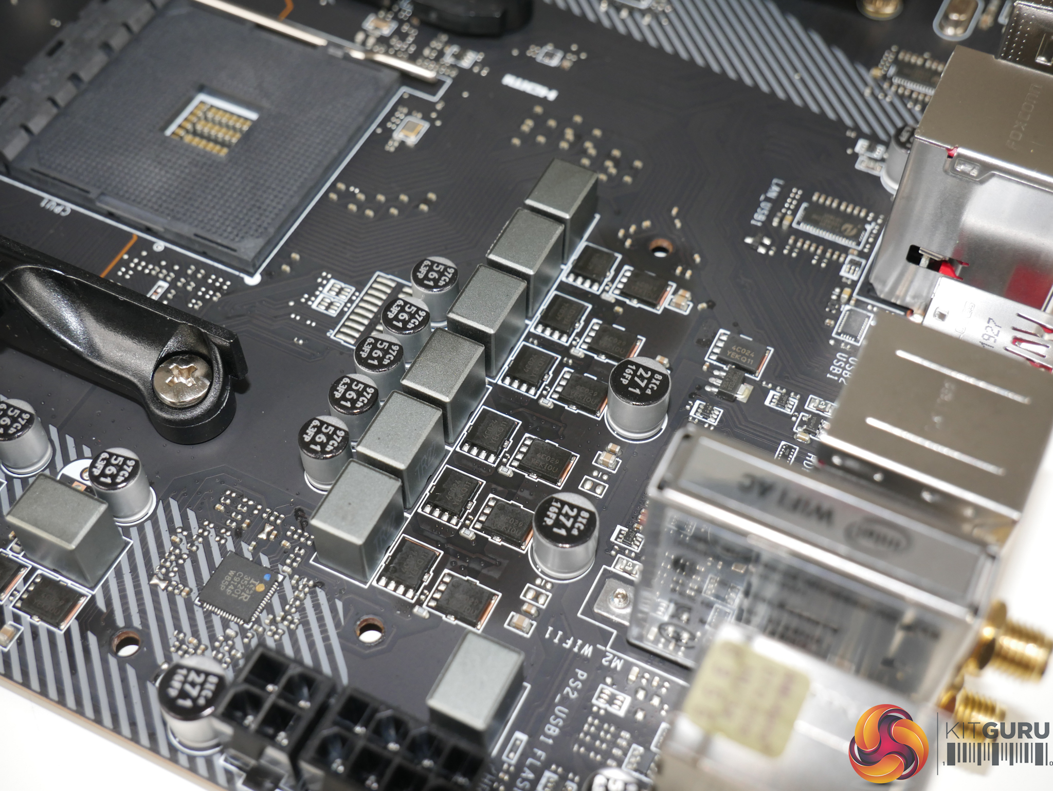
ASRock’s roughly £210 competitor comes in the form of the X570 Steel Legend. This motherboard features a unique and interesting design style, with camo-type patchwork on the PCB.
Focusing on the power delivery system, ASRock equips this motherboard with an 8+2 phase physical implementation.


ASRock is using an Intersil ISL69147 which is a dual output digital PWM controller that supports up to seven total control phases in an X+Y configuration. ASRock uses this capability, with the assistance of four ISL6617A phase doublers, all of which are mounted on the rear of the PCB in an un-cooled position.
The combination of ISL69147 PWM controller + four ISL6617 phase doublers gives ASRock’s X570 Steel Legend an electronic VRM system of 4×2 + 2. So, the CPU VCore VRM is made up of four doubled phases while the SoC VRM gets two dedicated phases without doublers.
Focussing specifically on the 4×2-phase CPU VCore MOSFET solutions, ASRock is using eight Vishay SiC634 DrMOS power stages. These co-packaged power stages are advertised with a 50A current capability for continuous output, though they do support a 10% higher current load for 10ms bursts. These are the same solutions that we have seen on ASRock’s higher-end X570 Taichi motherboard.
Overall, they’re pretty decent units and I would not call them out of place on a £210 mainstream motherboard. Importantly, for this test, the integrated power stages look to have a solid thermal resistance rating which should help when trying to shed their electrical resistance heat.
The two-phase SoC VRM is handled by a pair of Vishay SiC632A integrated power stages. These look to effectively be de-rated SiC634 solutions, with many of the specification curves highlighting a 45A realistic limit. These should be perfectly adequate for pushing the SoC, even when an APU is used.

Worth noting briefly is ASRock’s use of 12K-rated capacitors in the CPU and SoC region. This is an improvement to longevity over the 5K-rated caps we’d typically see on motherboards trying to squeeze the budget for their respective platform. It’s quite important in this scenario too, as the nearby heat from the VRM and high core count CPU can drive up capacitor temps and push them closer to that 105C rating level where the printed number of hours (5,000 or 12,000, for example) is a genuine statistical reality for expected operating life.

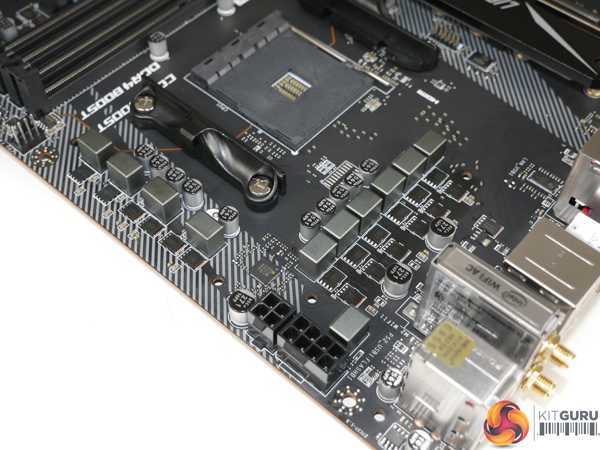
In terms of MOSFET heatsinks, I’d say ASRock’s effort is pretty poor. The two discrete heatsinks are more of a fashion accessory rather than real heatsinks as they feature very little effort to increase their surface area. There are some cut-outs here and there and a through-channel does help to increase surface area a little, but there’s no real sign of fins or genuine good heatsink design practice. At least the mounting pressure is good thanks to the use of screw fittings, and ASRock doesn’t overdo the thermal pad thickness which is good to see.


To an extent, inefficient heatsink design can be counteracted by simple metal mass. ASRock hasn’t really applied this logic, either, with the top-side SoC heatsink weighing 61 grams and the left-side CPU VCore heatsink weighing 82 grams.
The distribution of heatsink weight is actually pretty important in ASRock’s design as all of the CPU VCore MOSFET heat will be dumped into the single 82 gram heatsink. Typically, we’d see the CPU VCore MOSFETs mounted to the left and to the top of the CPU socket, thus splitting their thermal load between heatsinks. That’s not the case on the X570 Steel Legend.
At least the height of ASRock’s heatsinks is somewhat positive. They’re not low-profile or flat, so it is likely that incidental airflow will at least interact with the metal, even if not significantly.
There’s no heatpipe connecting the two heatsinks to one another, or to other heat-producing components such as M.2 SSDs or the X570 chipset. That means that the small blocks of metal are simply tasked with handling cooling for their MOSFETs mounted beneath, and nothing else.

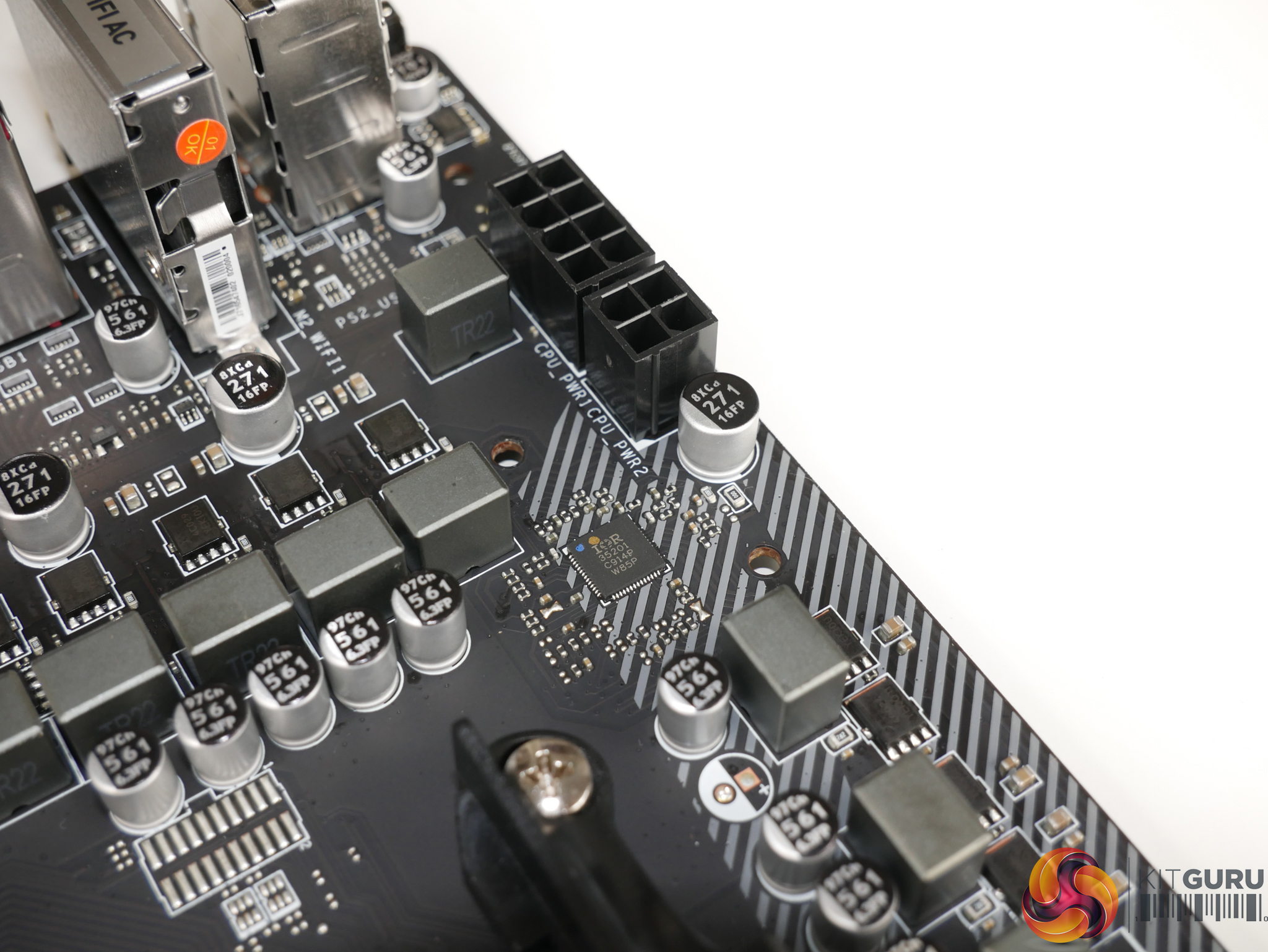
Finally, you get a supplementary 4-pin power connector partnering the 8-pin. That’s not really important for AM4 with a motherboard of this calibre.
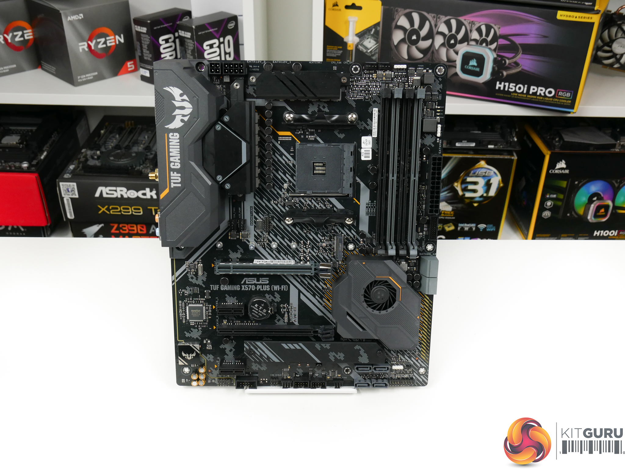
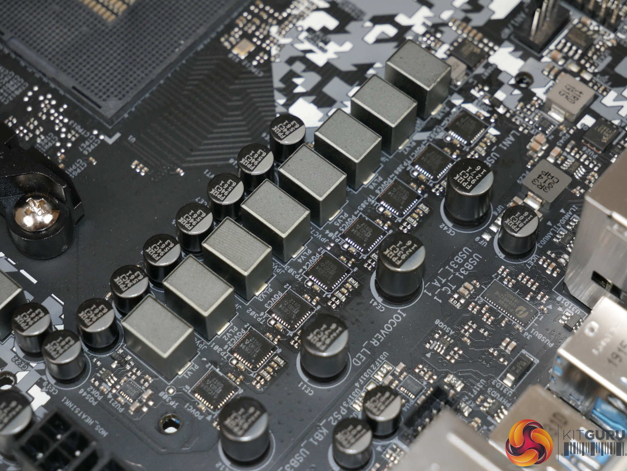
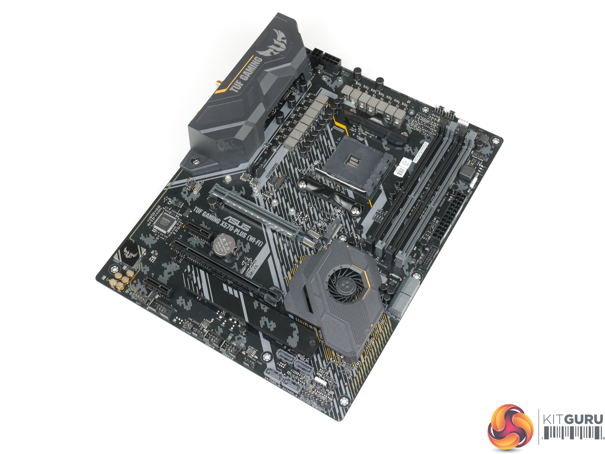
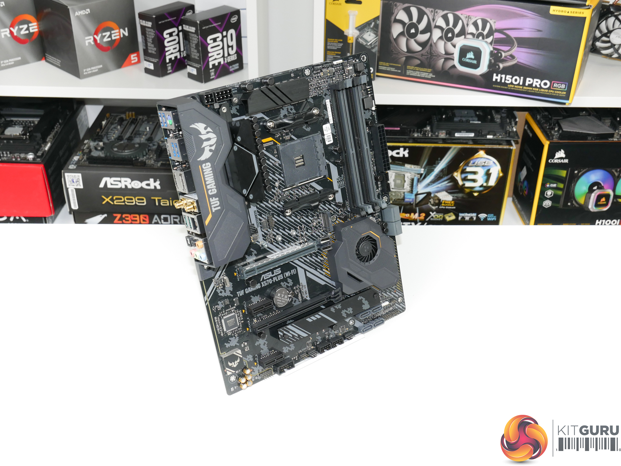
ASUS’ £210 competitor comes in the form of the TUF Gaming X570-Plus Wi-Fi – a name that is far, far too long! Technically, we have the £225 Wi-Fi version of this motherboard, but ignoring the wireless adapter makes it the £210 version. We checked with ASUS and they confirmed that there is no power delivery difference between the £225 Wi-Fi version and the £210 non-Wi-Fi alternative. So, we have no problem including this with our £210 competitors.
Here we see another motherboard that features camo-style design work on the PCB, in addition to ASUS’ usual yellow and grey accents for TUF series products.
Focusing on the power delivery solution, ASUS equips the TUF X570-Plus with a 12+2 phase physical implementation.
ASUS is using a proprietary ASP1106G PWM controller in a 4+2 phase mode. Details for this controller are limited but it is likely a re-badged Intersil PWM.
Interestingly, given the rather limited 4+2 electrical phase control capability of the PWM, we do not see ASUS applying any PWM phase doublers. This is typical of what we have seen from ASUS motherboards recently, with the vendor arguing that ‘fattening up’ the quantity of electrical components per phase signal is more beneficial than doubling the phases via a dedicated logic IC.
As such, ASUS’ 12 CPU VCore phases are actually a 4×3 design with three lots of electrical components per single control phase. You can see which phases are working together by decoding the text on the PCB highlighting power phase mounting positions.
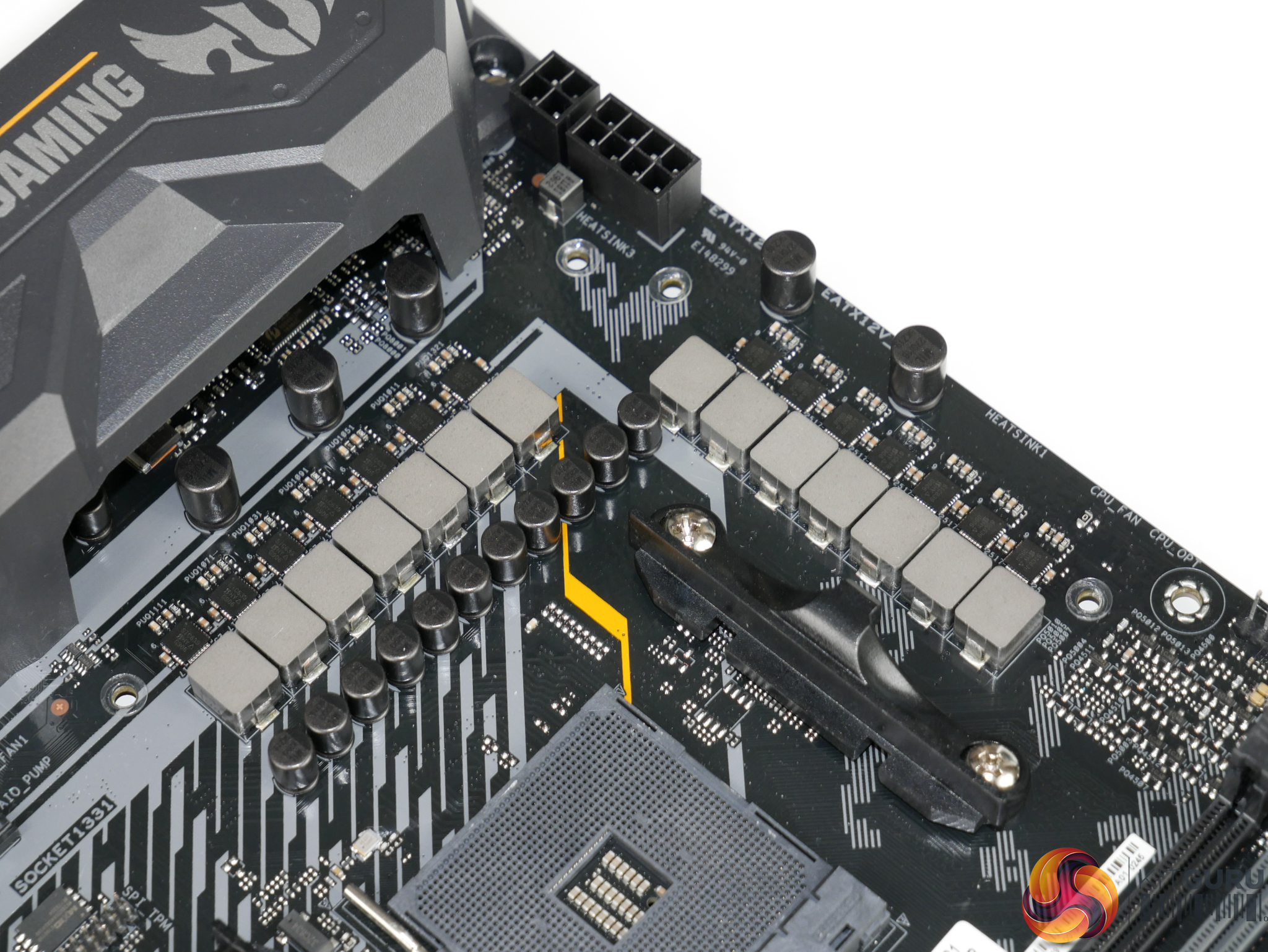
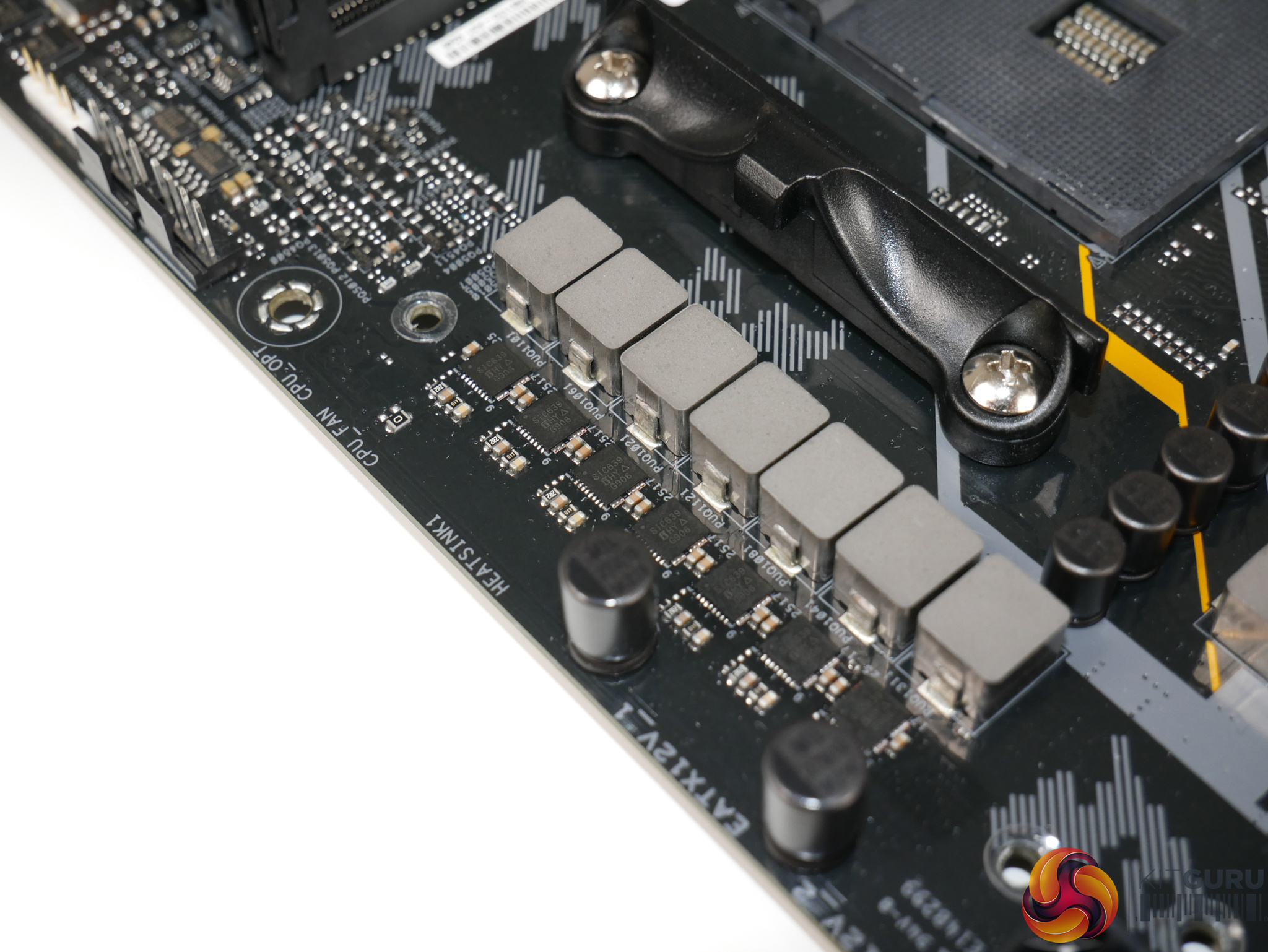
Focussing specifically on the 4×3, non-doubled CPU VCore power delivery system, ASUS is using a total of twelve Vishay SiC639 DrMOS power stages. These power stages are rated at ‘up to’ 50A of continuous current output just like we see from the SiC632 solutions and they look to be very slightly de-rated compared to the SiC634 alternatives.
Digging deeper into the spec sheet, the SiC639 looks to feature more focus on thermal monitoring compared to the SiC634 packages found on competing motherboards. The electronic block diagram shows an in-built thermal monitoring and warning function that features in the control loop. Either way, the SiC639 power stages look to be good solutions for a £210 AM4 motherboard, especially with the quantity of physical phases that ASUS deploys to balance the overall CPU load.
The two SoC phases uses the same SiC639 power stages and each electronic phase gets one power stage, not three like we see for the CPU VCore VRM. Rather than split the SoC VRM phases off into their own PCB section, ASUS deploys them on the top-left corner of the of the bank of 14 physically mounted phases.
Capacitor-wise, ASUS is using 5,000 hour rated ‘Black Metallic TUF caps’. While the headline 5,000 hour figure of these capacitors is pretty basic for a £210 motherboard, ASUS’ marketing material highlights an operating temperature of up to 125°C for the 5,000 hour rating. This is important, as the exponential-style curve will mean that the lifespan is mathematically likely to be higher than 5,000 hours at the usual rating temperature of 105°C. The operating life will be even longer when realistic running temperatures of 80°C or below are used.
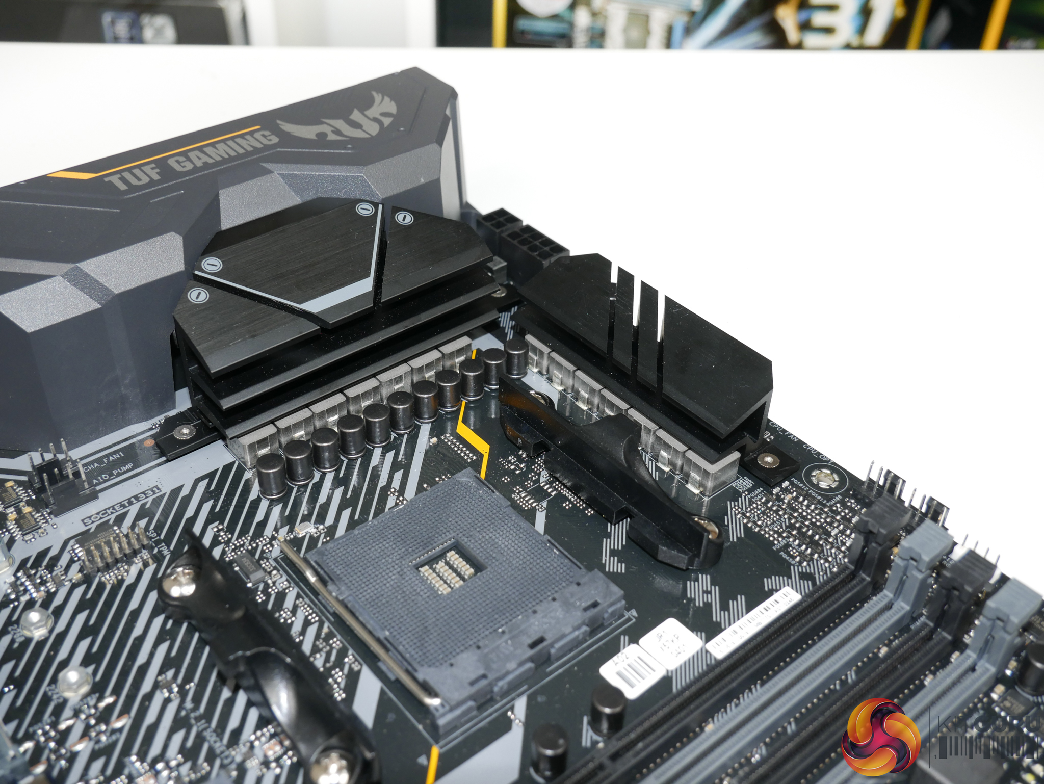

ASUS is clearly banking on efficient operation from the twelve physical CPU VCore VRM phases as the heatsinks deployed are poor. There’s no real effort to increase surface area in the direction of airflow by using fins. You get a few tiers or cut-outs on both of the metal heatsinks, but I wouldn’t say that significant effort has been put into designing an efficient heatsink. This is more of an aesthetic heatsink.
With that said, mounting pressure is strong thanks to the use of screws as a securing mechanism. The applied thermal pads also look to be well-specced and clearly aren’t too thick for their purpose.
ASUS actually deploys an additional thermal pad compared to what we’re used to see. This contacts the top of the inductors in an effort to draw heat away from them. How much use this will be is hard to say, as we don’t typically see thermal problems from chokes thanks to their higher surface area compared to MOSFETs helping them dump heat. Perhaps ASUS is thinking about motherboard comparisons using thermal imaging, at which point direct heatsink contact and therefore lower inductor temperature may show up as a positive.

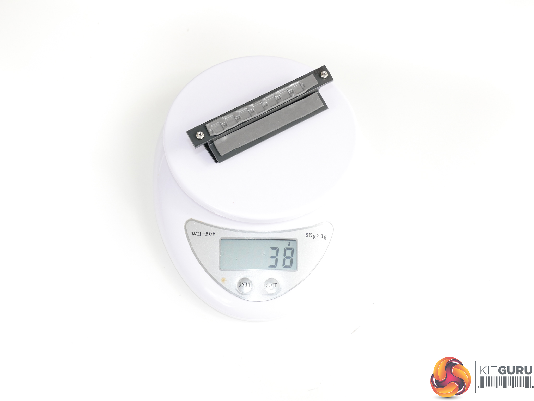
Weight wise, the left side VRM heatsink comes in at 75 grams while the top heatsink is a measly 38 grams. Again, ASUS looks to be banking on electrically efficient operation of the power stages to allow the small heatsinks to prove fit for purpose.
Compared to ASRock’s competitor, which has a higher mass of heatsink in total, ASUS actually has more heatsink mass allocated to the CPU VCore thanks to the mounting design. With six CPU power stages split to the left of the AM4 socket and six more above it, the two heatsinks are each tasked with cooling the CPU VRM MOSFETs, as opposed to just one of the heatsinks. This is a better design than ASRock’s bunched formation as it also allows thermal load from the power stages to be split across a larger area of the PCB, thus mitigating specific hotspot areas.
One area where ASUS deserves credit on this £210 X570 motherboard is the use of a six-layer PCB. The higher layer count should help to manage heat load into the PCB.
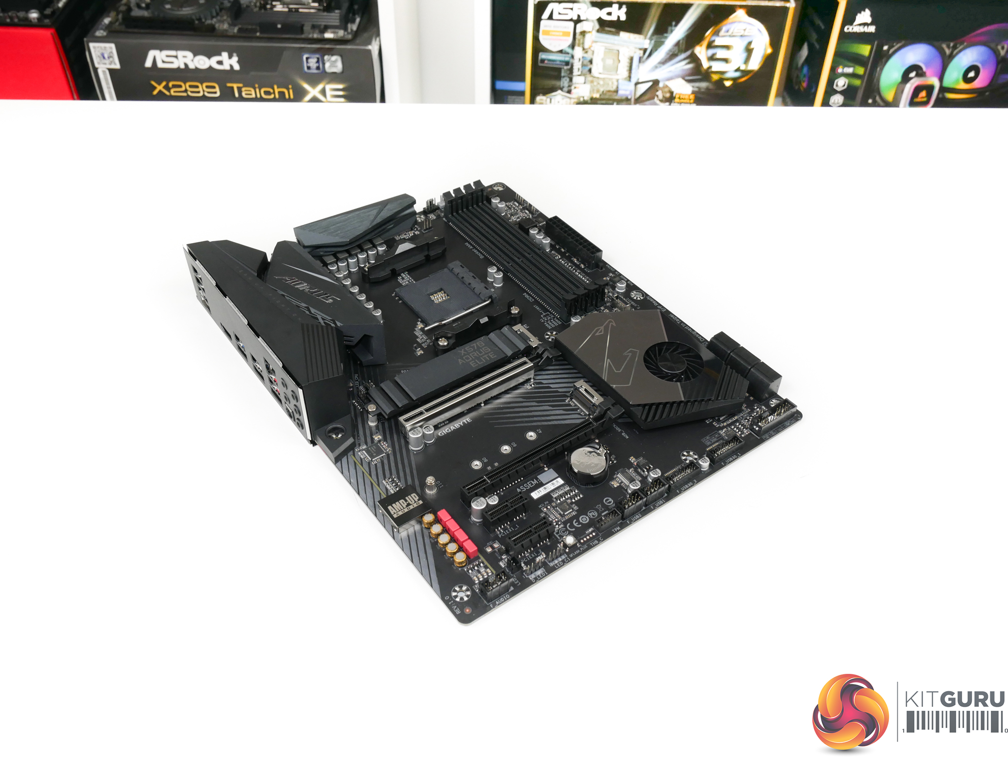
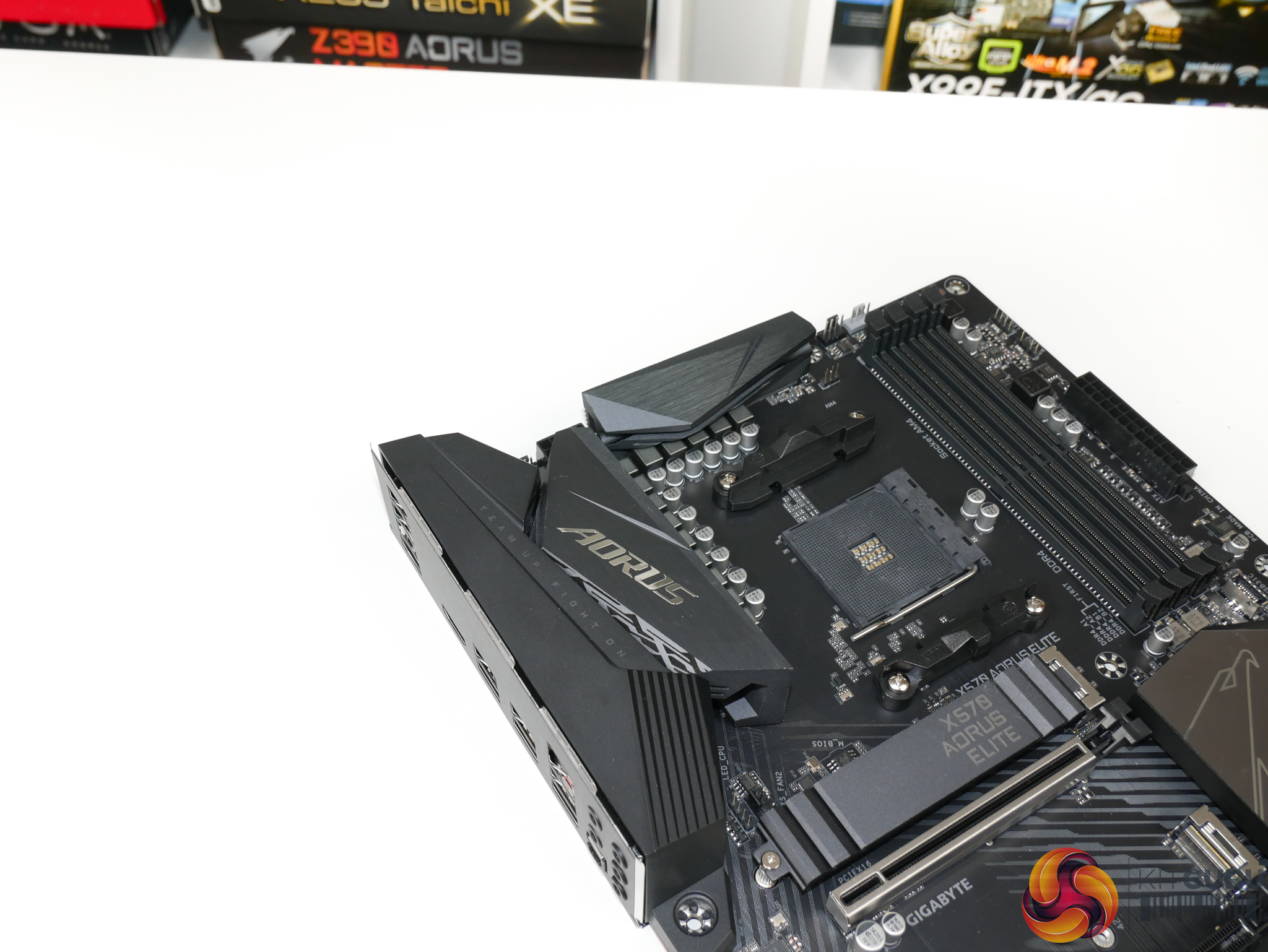
Gigabyte’s £210 competitor comes in the form of the X570 Aorus Elite. Gigabyte deploys the typical Aorus motherboard colour scheme of dark greys and blacks which looks pretty good in my opinion.
Focusing on the power delivery system, Gigabyte equips this motherboard with a 12+2 phase physical implementation.
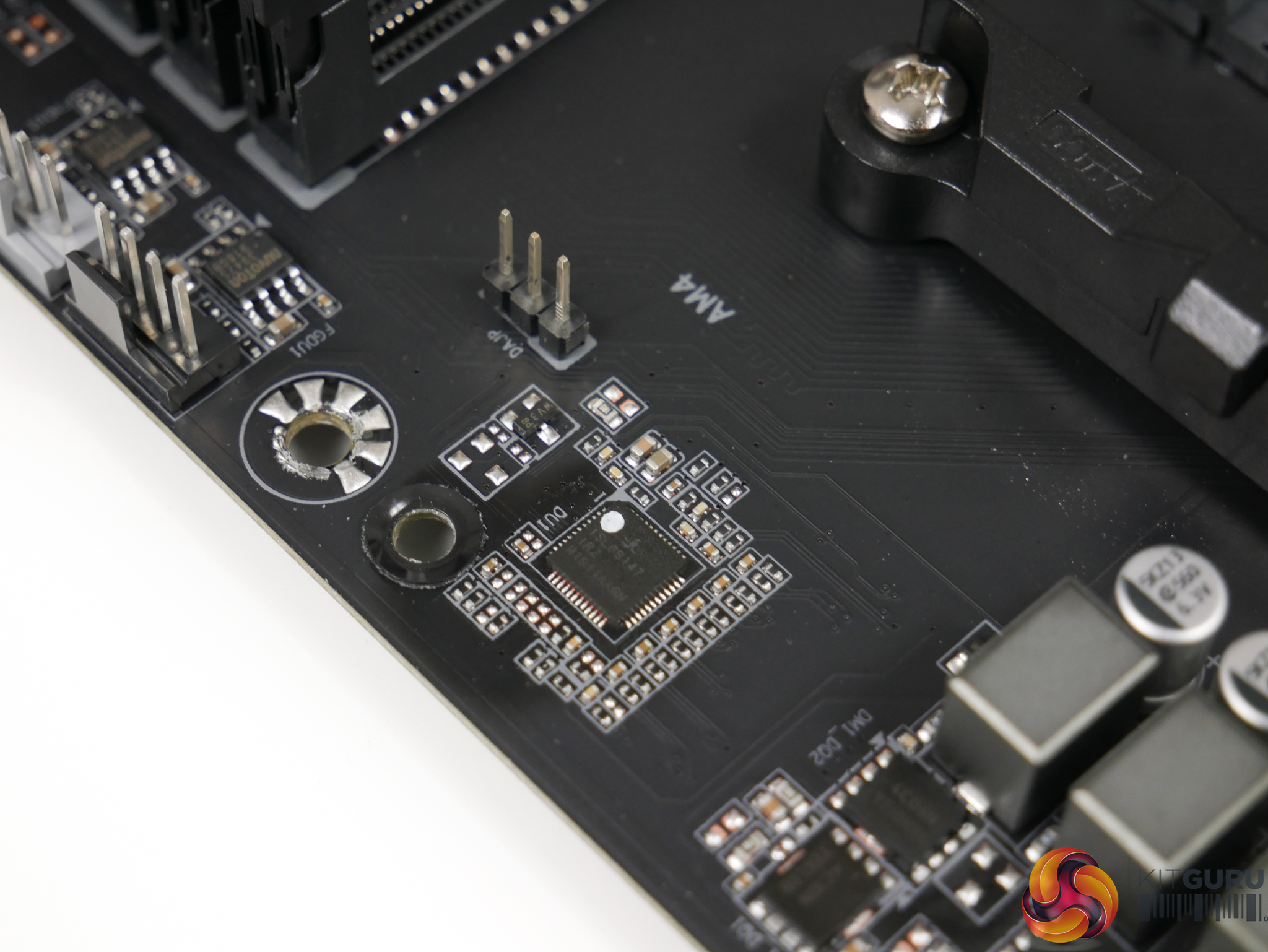
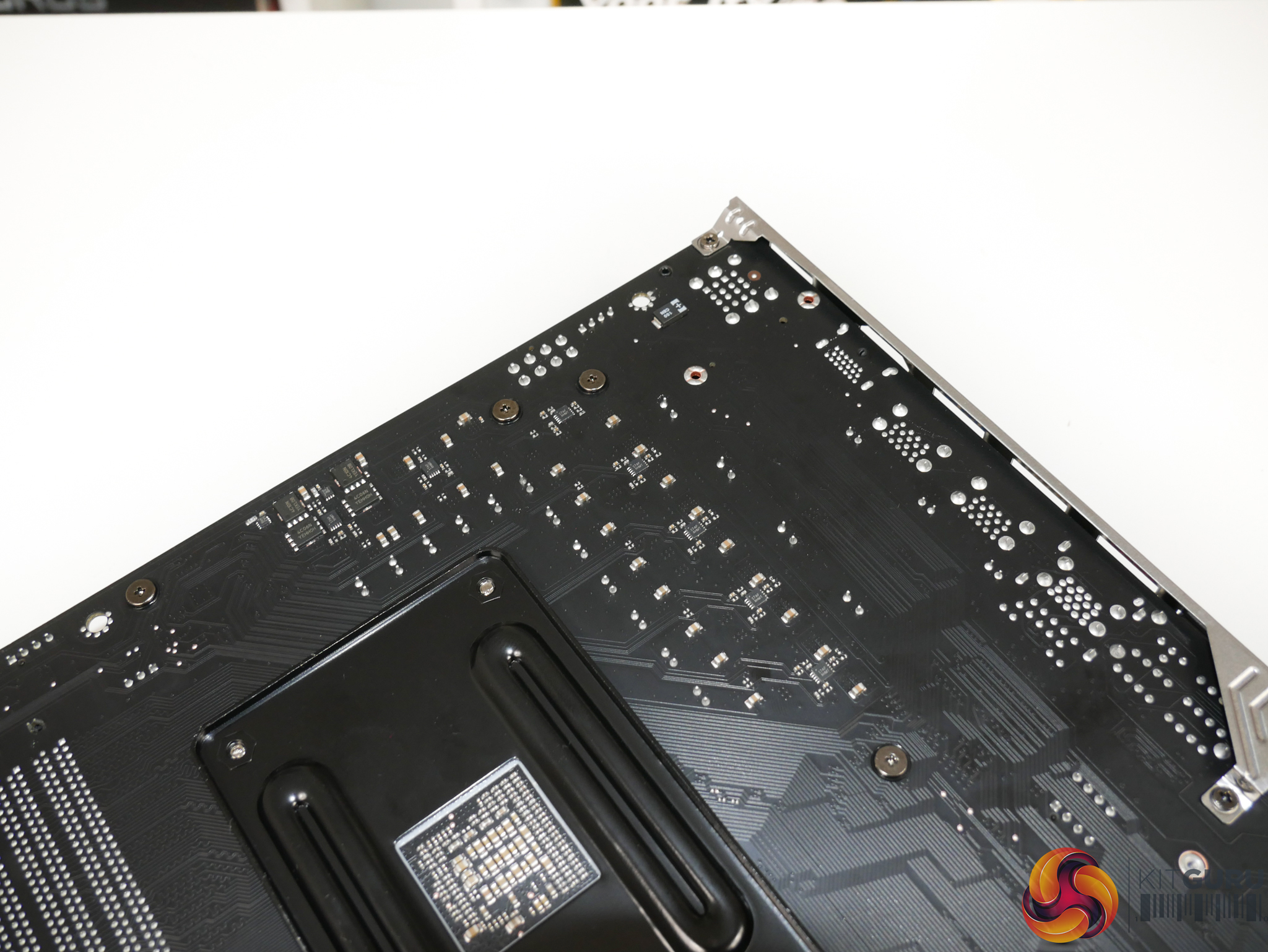
Gigabyte is using the same Intersil ISL69147 PWM controller as ASRock. Again, this is a dual output digital PWM controller that supports up to seven total control phases in an X+Y configuration. With Gigabyte, however, this seven-phase capability is utilised with the assistance of seven ISL6617A phase doublers, all of which are mounted on the rear of the PCB in an un-cooled position.
The combination of ISL69147 PWM controller + seven ISL6617 phase doublers gives Gigabyte’s X570 Aorus Elite an electronic VRM system of 6×2 + 1×2. So, the CPU VCore VRM is made up of six doubled phases while the SoC VRM gets one doubled phase.
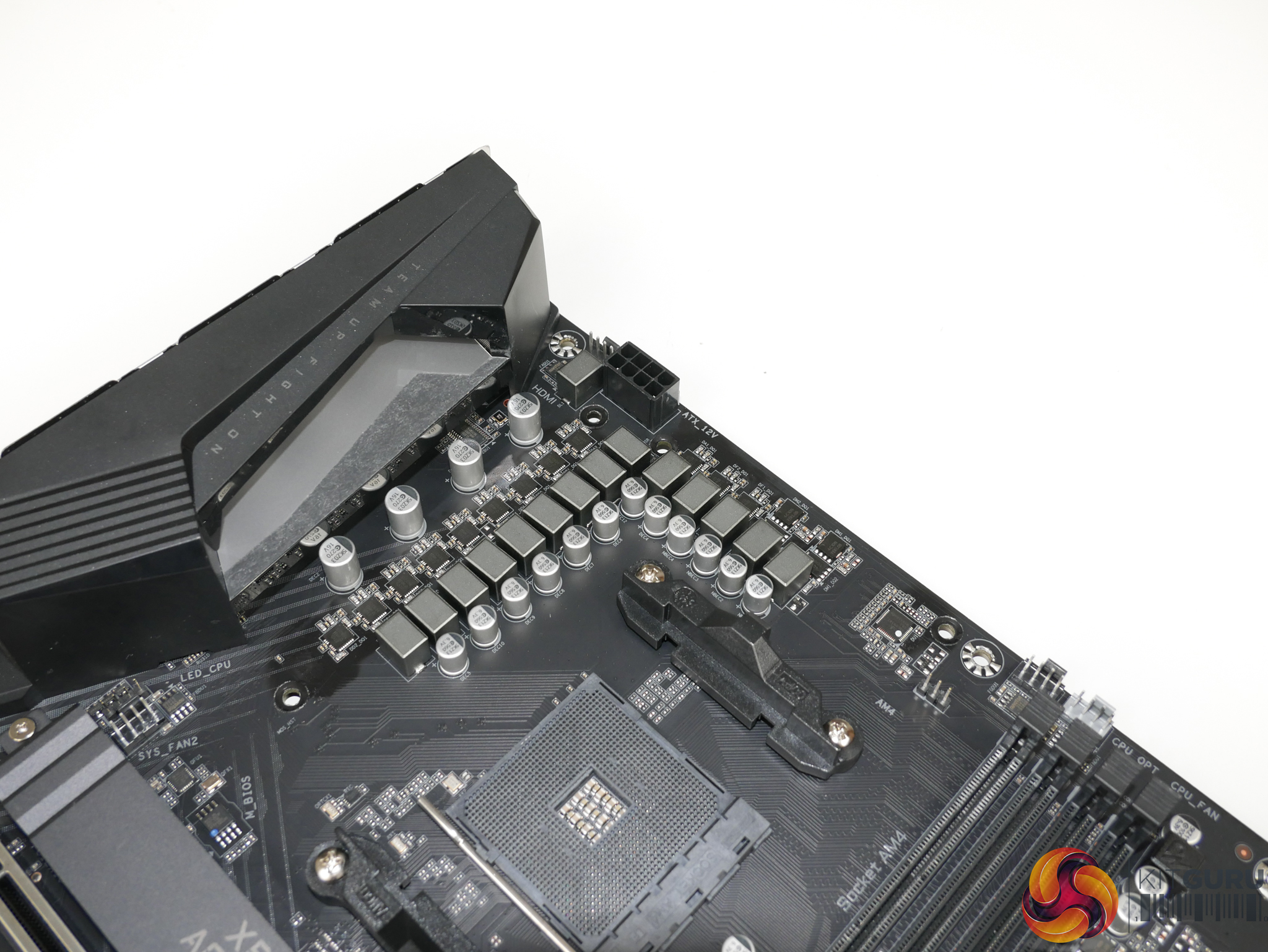
Focussing specifically on the 6×2-phase CPU VCore MOSFET solution, Gigabyte is using the same Vishay SiC634 DrMOS power stages as ASRock. Gigabyte, however, deploys a total of twelve power stages compared to ASRock’s eight. Just in case you forgot the numbers since our ASRock reference, these co-packaged power stages are advertised with a 50A current capability for continuous output, though they do support a 10% higher current load for 10ms bursts. As we have already mentioned, these are solid power stages to use on a £210 X570 motherboard, especially when Gigabyte is deploying a dozen of them specifically for the CPU VCore VRM.
The 1×2 phase SoC VRM is driven thanks to one PWM signal from the Intersil controller and the use of a doubler.

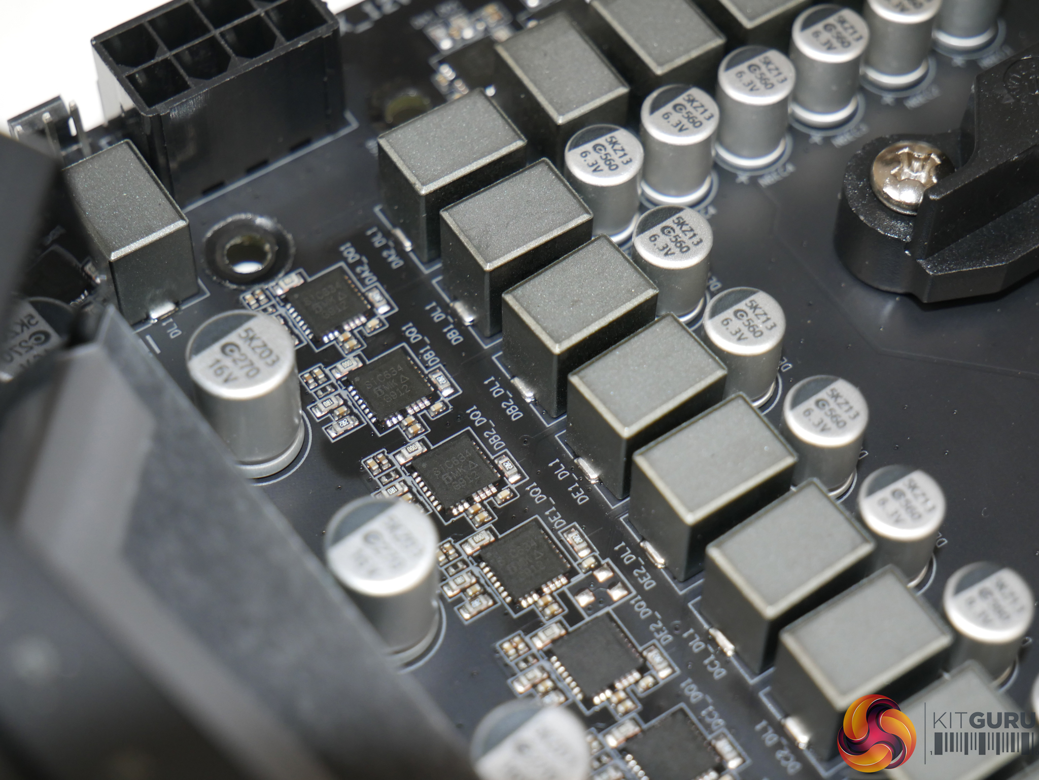
Gigabyte deploys basic On Semi 4C06N and 4C10N high- and low-side MOSFETs to drive the SoC VRM. Despite being one PWM signal doubled to two electrical phases, Gigabyte doubles this again to make four physical phases worth of electrical components. This can be viewed as a fat, doubled, two phase design. Four 4C06N MOSFETs are used with two on the front and two on the rear. The exact same mounting is used for the four 4C10N MOSFETs. As the On Semi MOSFETs are not DrMOS solutions – they’re effectively ‘dumb’ FETs – Gigabyte is also forced to deploy two Intersil ISL6625A driver ICs on the rear.
The SoC VRM is undeniably basic in terms of electrical component quality. However, this is likely to be a non-issue for most X570 users who will be running with a dedicated graphics card.
Assessing the CPU VCore alone, Gigabyte’s 12-phase doubled solution is practically identical to that used on the £300 ASRock X570 Taichi. That’s a clear positive for Gigabyte’s £90 cheaper board.
One area where Gigabyte looks to have gone for a basic component representative of this board’s price tag is with the capacitor choice. The 5,000 hour rated capacitors are likely to be fine for almost all situation when the extended lifespan at lower running temperatures is accounted for. However, both ASUS and ASRock look to be using higher-rated alternatives that may be slightly be for longevity… if you plan to keep this board pushed hard forever … which you shouldn’t.
Also worth noting is that Gigabyte provides a single 8-pin CPU power connector. But that simply won’t be an issue unless you opt for extreme cooling solutions on the CPU.
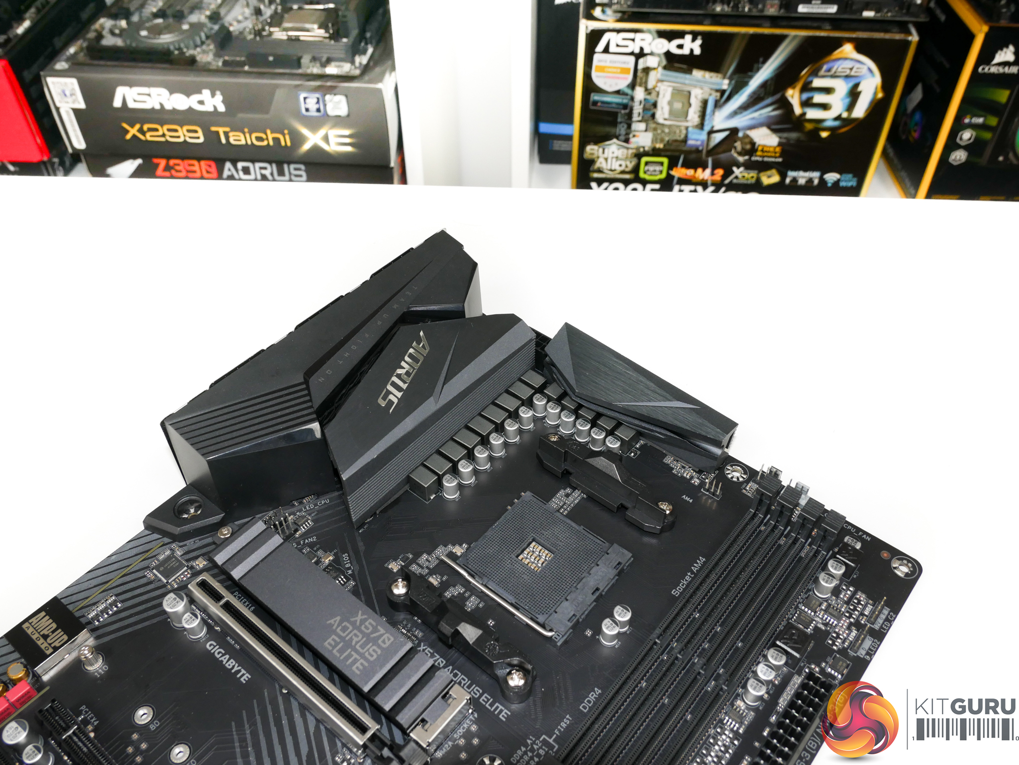
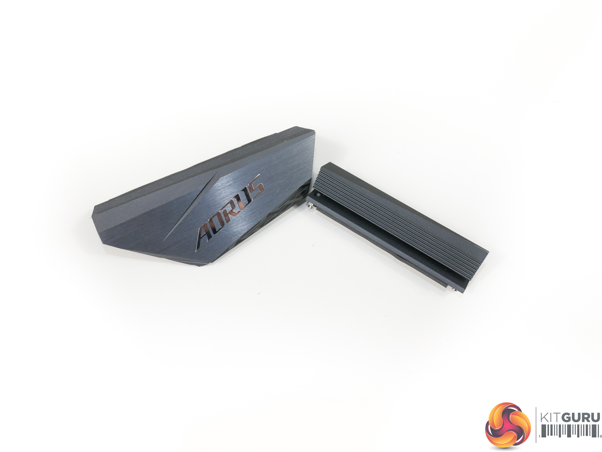
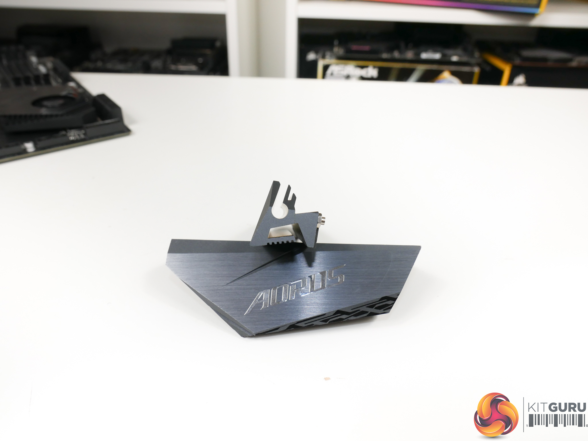
Continuing the heatsink trend, Gigabyte designs the X570 Aorus Elite’s heatsinks with more focus on design than cooling performance. There’s no real attempt to increase surface area by using vertical fins. With that said, a similar approach to ASUS is applied where the heatsink is somewhat split into tiers in a small effort to increase surface area.
Mounting pressure is good thanks to the screw fit and the thermal pad looked to be of an appropriate thickness.
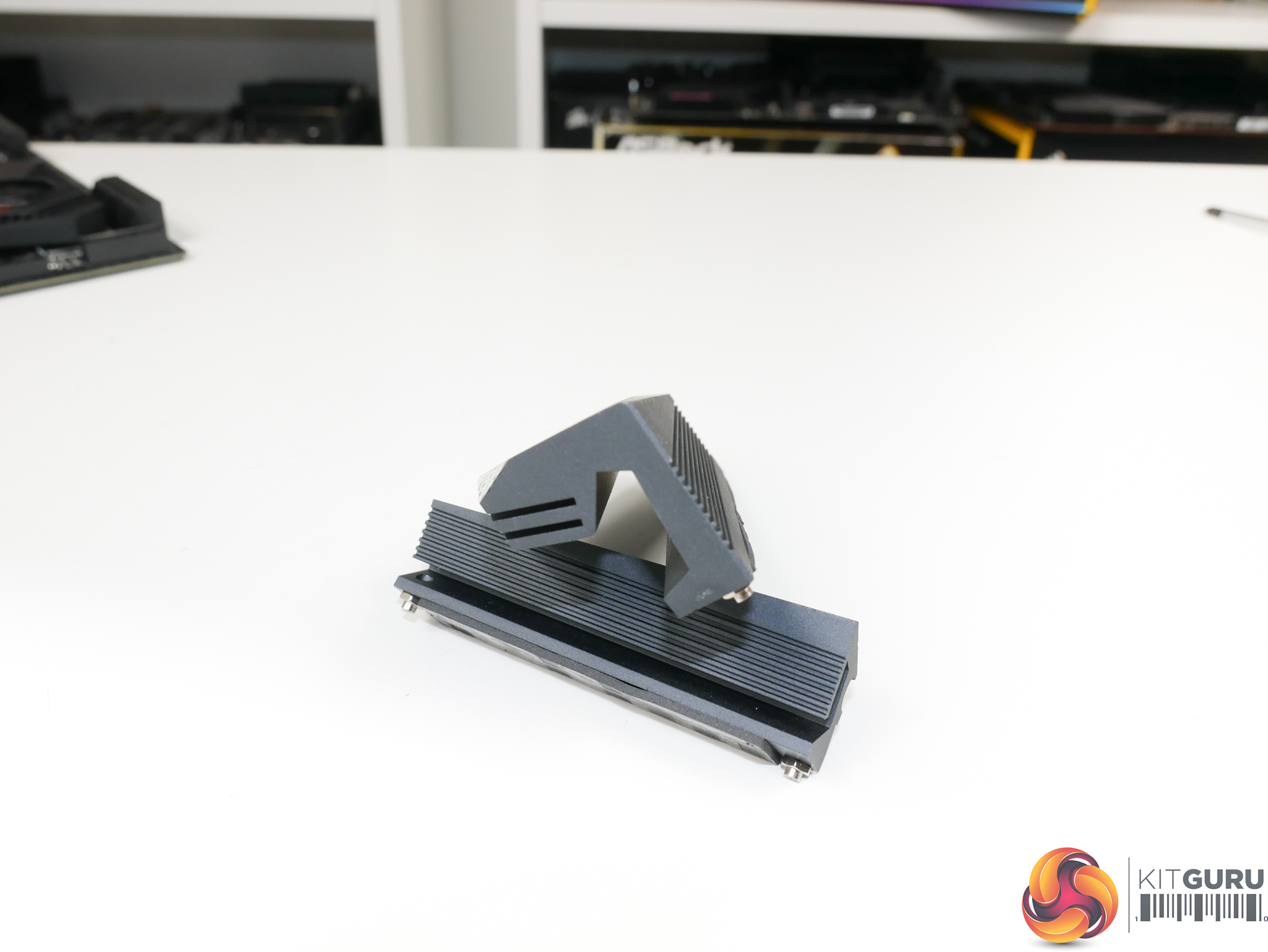
The larger left-side heatsink weighs 133 grams while the smaller top heatsink is 60 grams. That roughly 2:1 heatsink mass split looks to be pretty smart as the heavier left-side heatsink is tasked with handling nine of the CPU VCore power phases while the smaller top-side heatsink manages three CPU phases and the two SoC phases.
Balancing the thermal load of the 12-phase CPU VRM across two heatsinks is a smart solution that ASUS also deployed. In Gigabyte’s design, the left-side heatsink will have to manage around 75% of the resistive heat output from the SiC634 power stages, while the top-side will deal with around 25%.
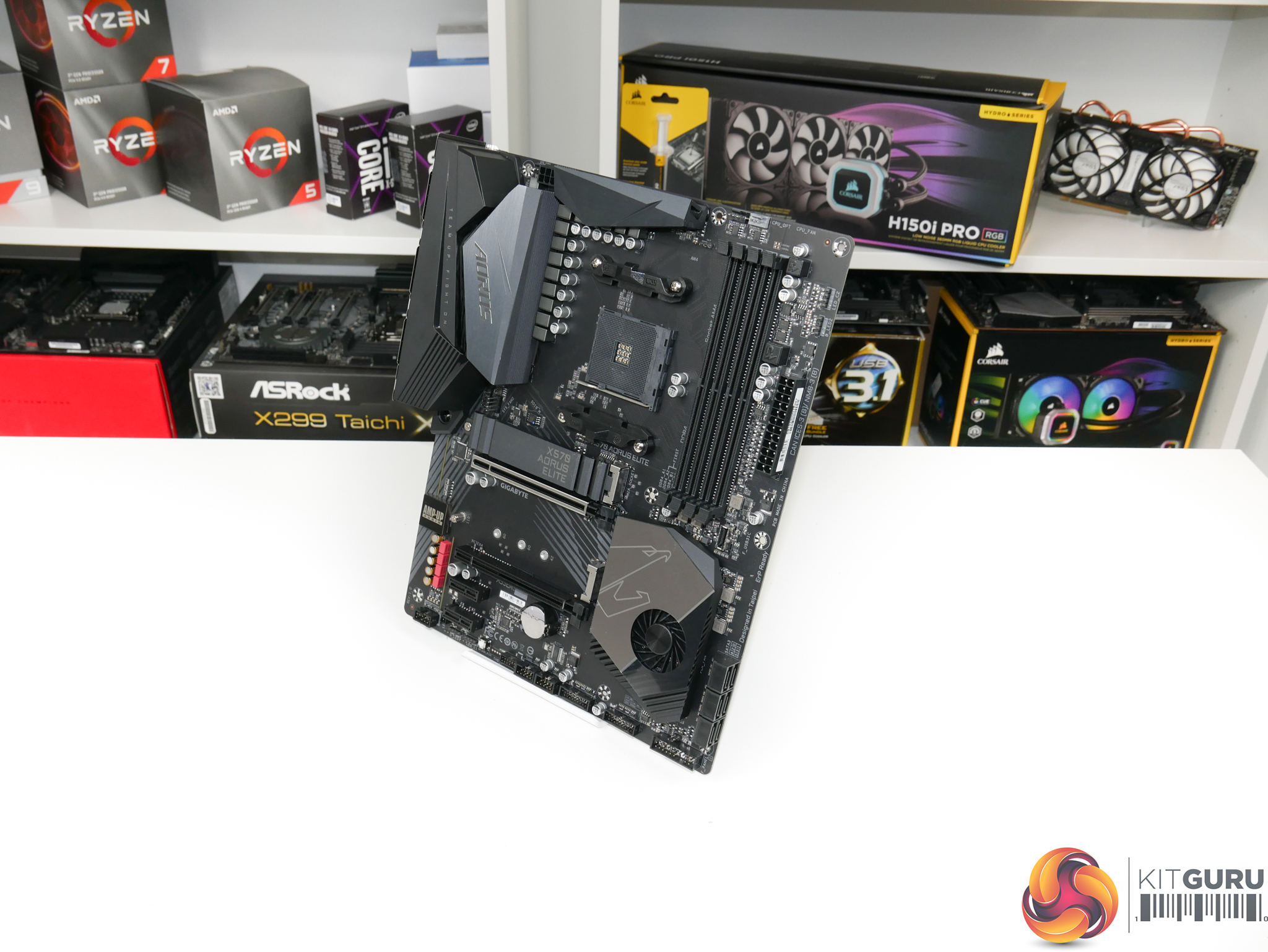
Gigabyte is using a 4-layer ‘normal loss’ PCB on the X570 Aorus Elite. That’s step-down from some of the higher-end offerings in Gigabyte own X570 line-up, and it isn’t quite as good as ASUS’ 6-layer.
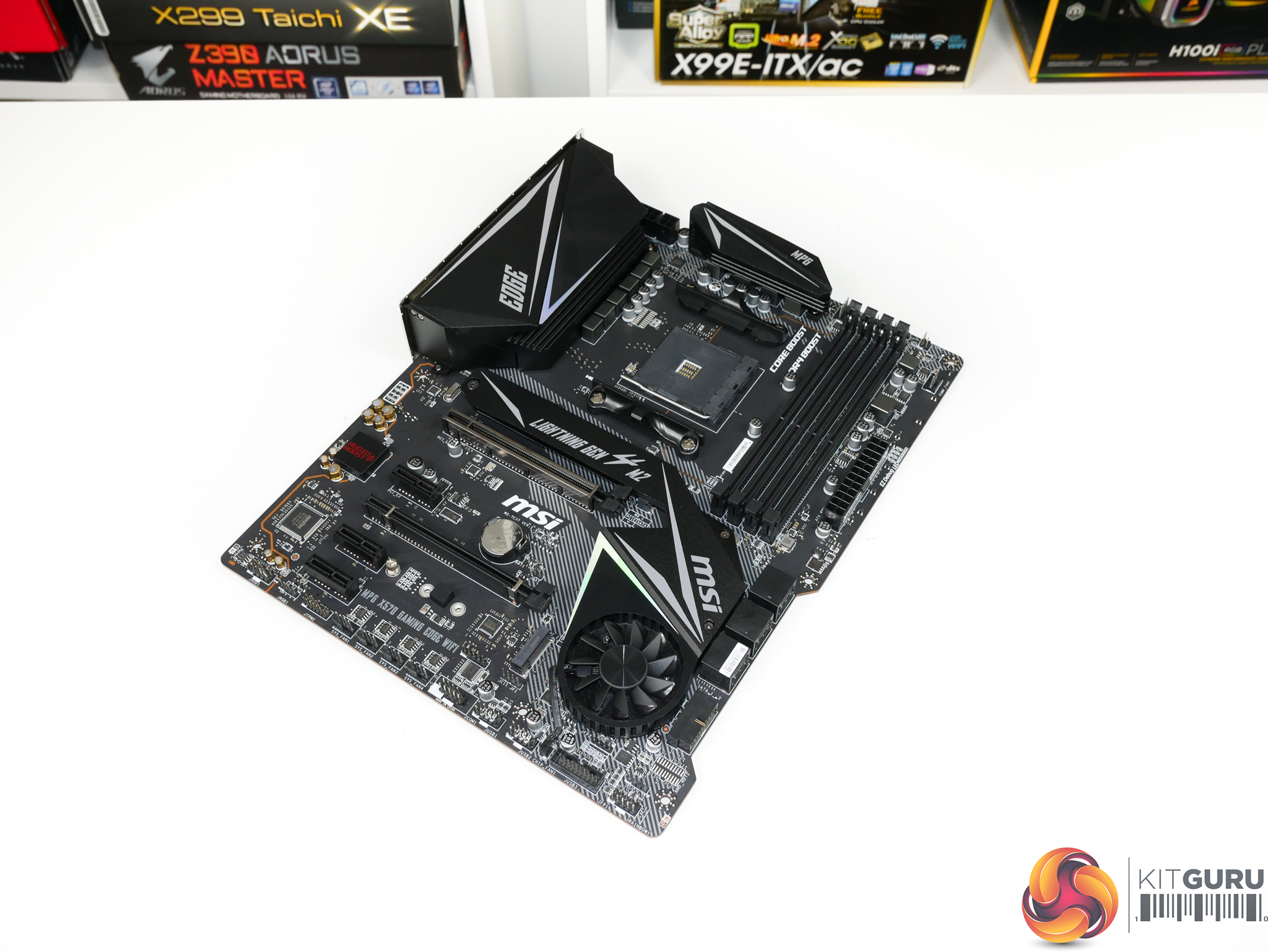
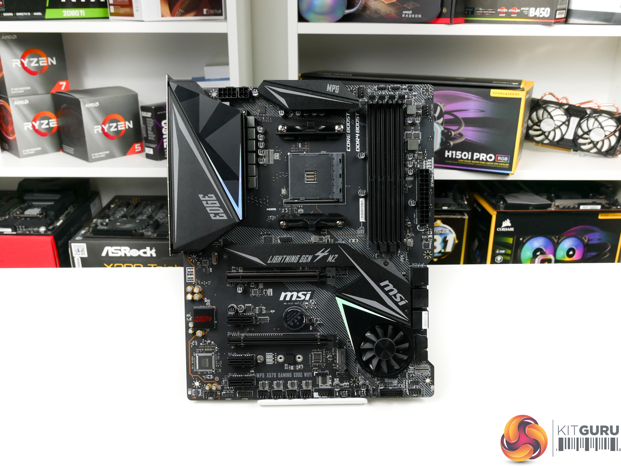
MSI’s £210 competitor comes in the form of the MPG X570 Gaming Edge Wi-Fi. Just like ASUS’ offering, this name is annoyingly long! MSI deploys the typical motherboard colour scheme of dark greys and blacks which looks pretty good in my opinion. A massive RGB lighting edge is one of the key features for MSI.
Focusing on the power delivery system, MSI equips this motherboard with an 8+2 phase physical implementation.
MSI is using the superb International Rectifiers IR35201 PWM controller in a 4+2 phase mode.
A total of five IR3598 phase doublers/dual drivers are deployed on the rear PCB. Four of these are used in doubler mode to double the four PWM phases allocated for CPU VCore and drive the eight sets of high- and low-side MOSFETs. The remaining IR3598 is deployed in dual driver mode to drive the two pairs of high- and low-side MOSFETs allocated for the 2-phase SoC VRM.
As such, MSI’s 8 CPU VCore phases are actually a 4×2 design and the SoC is a pure 2-phase design.
Focussing specifically on the 4×2-phase CPU VCore MOSFET solution, MSI is using 4C029N and 4C024N High- and low-side MOSFETs from On Semi. A total of eight of these pairs are deployed, so this VRM solution would be most closely matched to ASRock’s 8-phase X570 Steel Legend.
With that said, the ‘dumb’ On Semi discrete MOSFETs are undeniably basic for a £210 X570 motherboard, they take up more PCB real estate than co-packaged power stage solutions, and there is a high likelihood of higher electrical losses simply by virtue of the high- and low-side MOSFETs being physically detached from one another. Their thermal resistance ratings aren’t great compared to the Vishay DrMOS power stages, either.
The 2-phase SoC VRM is made up of two pairs of discrete MOSFETs. I could not find details about these solutions as the writing is unclear and the model is uncommon. These are driven by the rear mounted IR3598 dual driver.
As was the case with Gigabyte, the SoC VRM is undeniably basic in terms of electrical component quality. However, this is likely to be a non-issue for most X570 users who will be running with a dedicated graphics card.
MSI provides an additional 4-pin power connector to supplement the 8-pin one. This isn’t necessary for a board of this calibre as you’re unlikely to saturate a single 8-pin.
Yet again, we see heatsinks with a design more focussed on aesthetics than cooling efficiency. For the larger, left-side heatsink, there are no fins or real attempts at designing in fins, other than a few ridges in certain locations. The top heatsink is clearly given a little more attention when it comes to surface area, with stacked ridges found on the front and back positions.
Mounting sturdiness is good thanks to the screw fit. The thermal pads applied by MSI looked to be thicker than those found on competing vendors’ solutions and they didn’t seem to be applying as much pressure to the MOSFETs, as judged by the minimal imprints when removing the heatsink.
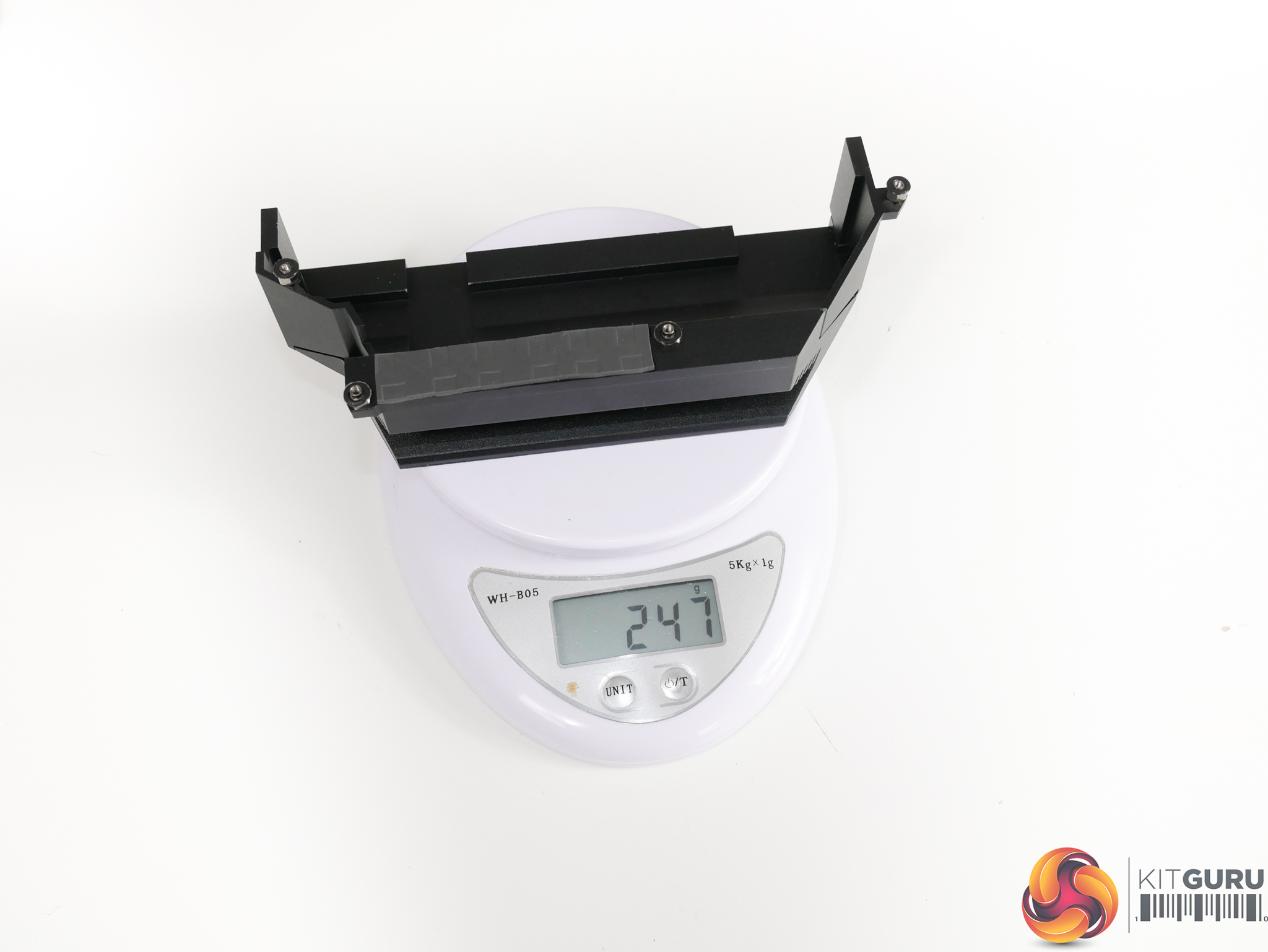
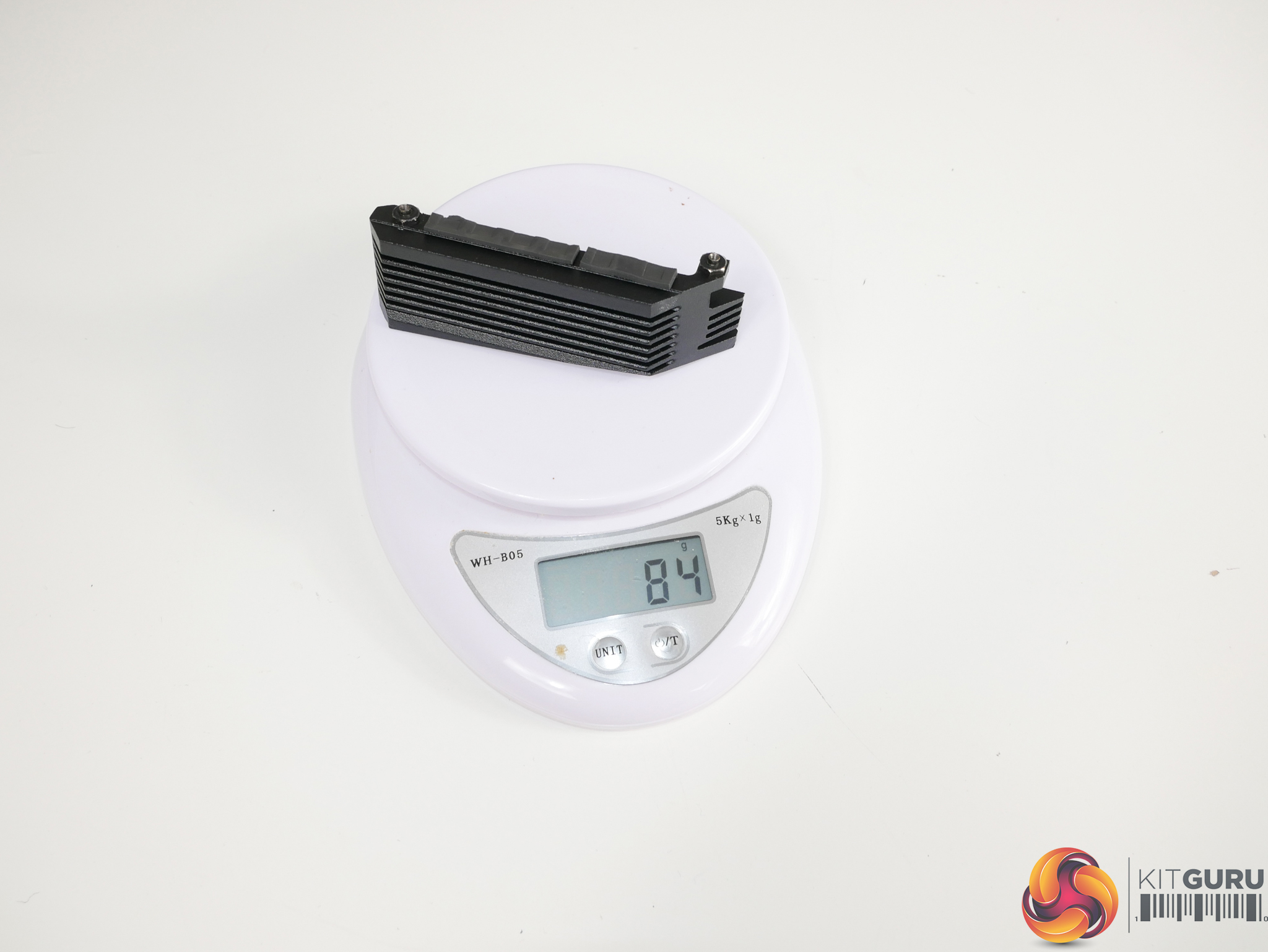
The larger left-side heatsink weighs a massive 247 grams while the smaller top heatsink is a solid 84 grams. Clearly, MSI is aiming for a brute force approach at dealing with the heat output from its less efficient MOSFET solutions.
That roughly 3:1 split for heatsink mass is pretty much ideal, as the larger left side heatsink is tasked with cooling six CPU power phases while the smaller top heatsink is given two phases to cool, plus the less-demanding SoC VRM.
If MSI’s heatsink design can remove the electrical resistance heat from the MOSFETs, there should be no concerns for reduced performance. That does, however, demand at least a decent amount of case airflow to interact with the metal cooling slabs.
While MSI’s heatsink design isn’t as efficient as it could be, there is a massive slab of metal with a relatively high amount of surface area via a brute force approach. This large heatsink will help to dampen any sudden changes in MOSFET temperatures when short, heavy loads are applied. But for sustained heavy loading, there still needs to be sufficient surface area for the heat to be dumped away from the metal block.
Overall, I’d say MSI has the best heatsink design of all four boards on test today, simply by brute force. Sometimes, there doesn’t need to be elegance to the approach – a big chunk of metal can potentially be a solid solution.
For performance testing, we will be running each of these boards using the flagship AMD Ryzen 9 3900X 12-core CPU. Upping the ante, we’ll be overclocking this power-hungry beast to 4.25GHz using around 1.35V, which results in a CPU power draw that closes in on 200W – certainly a hefty task for affordable X570 motherboards.
The latest non-ABBA AGESA BIOSes were used on each board. We have seen bugs with most of the AGESA ABBA BIOSes that make Ryzen Master readings completely incorrect. As such, we stuck to the ABB BIOSes for this testing, which is fine as we were not using Precision Boost 2 or PBO.
A Note on Voltages
As voltage accuracy and load-line calibration settings are different between the motherboards, we have applied a couple of techniques to make sure our CPU voltage is kept as close as possible to our 1.35V target.
With ASRock and ASUS, this meant adjusting the load-line calibration to get a software-read voltage reading close to 1.35V. We checked the power consumption from the wall to act as a validation check (as some software readings for package power are incorrect). For the Gigabyte X570 Aorus Elite, we had to drop the voltage slightly and adjust the LLC to get to 1.35V under load.
With MSI’s MPG X570 Gaming Edge WiFi, the software-based voltage readings do not seem to be accurate. This board drew as much as 35W more power from the wall despite reading the same 1.35V voltage as other boards. We dropped the voltage slightly to try to compensate for this and to bring the wall power closer to the competing motherboards. However, the board still drew slightly more power than the competitors by around 5-15W.
Test Procedure:
Our load test case uses 1 hour of continuous full load using AIDA64. We take temperatures readings at the end of the sustained 1-hour load, ensuring that no major thermal throttling or VRM throttling has occurred throughout the specific test run.
Temperature Measurement Procedure:
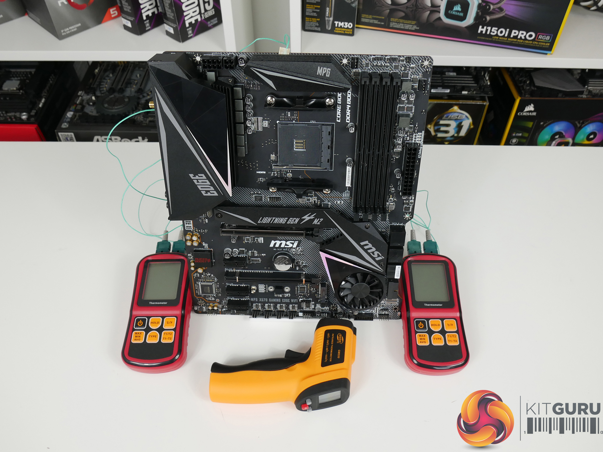
- We primarily use several K-type thermocouples mounted in specific locations on the motherboard to measure temperatures. Our preferred mounting positions were:
- Left side MOSFET bank at the bottom
- Left side MOSFET bank in the centre, which is the likely hottest spot
- Top MOSFET bank in the centre (where possible)
- Rear PCB, directly beneath the left-side central MOSFET
- We additionally did some validation checks by mounting on the front-side PCB directly adjacent to the left-side inductors, and also whilst mounted on the heatsink if necessary.
- As we were mounting the thermocouples directly to the MOSFET surfaces in many of our test cases, we decided to opt for flat constructed K-type thermocouples, rather than the common ‘ball-ended’ ones.
- These flat thermocouples featured a wire loop that was covered by a thin package of Kapton tape. The relative thinness of this packaging solution meant that there should be minimal interference to heat flow through to the VRM heatsink and the loop design allowed us to cover the MOSFET package surface.
- Another tool that we used was our simple hand-held laser thermometer for additional checks to PCB temperatures. This was used when the PCB had minimal reflectivity so that emissivity concerns when using this form of measurement technique could be minimised.
- We decided against using thermal imaging as we were most interested in MOSFET surface temperature with the heatsink in place, so thermal imaging would just show us heatsink temperature, which is not necessarily representative of design efficiency, performance, or underlying MOSFET temperature. Equally so, our surface measurements techniques for the PCB temperature were deemed adequate for our testing.
One of the key challenges was minimising the effect that electromagnetic interference (EMI) had on our thermocouple readings. This was especially challenging when we were forced to route the thermocouples close to capacitors or inductors.
We aimed to mitigate this issue by spot-checking PCB temperatures with the laser thermometer as a validation check. We also decided to cross-reference with software readings where they were available. And we checked temperatures with the load applied and with all power to the system killed, thus showing EMI-free readings just a few seconds after the load is removed but with heat still in the system.
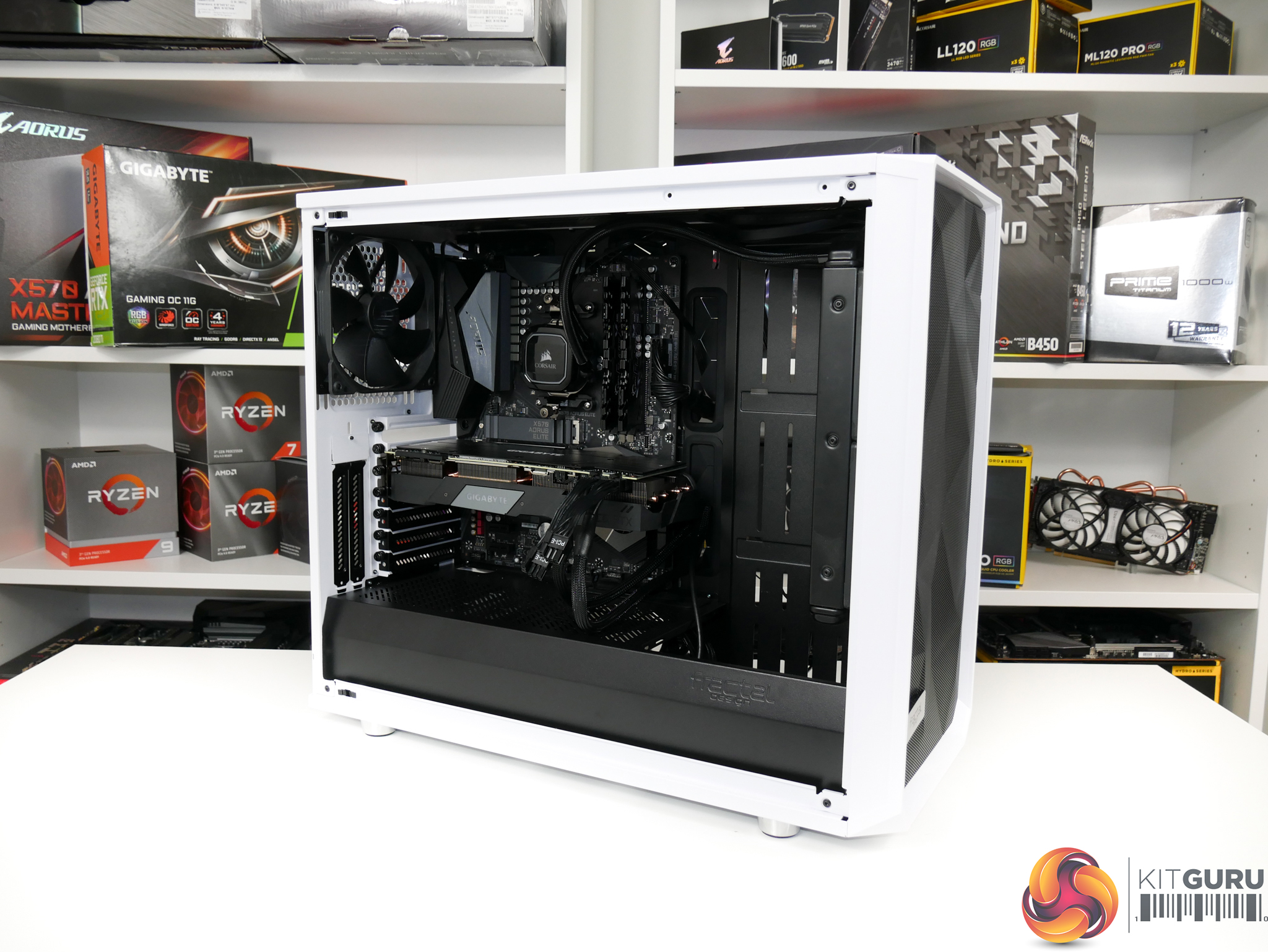
X570 Test System:
- Processor: AMD Ryzen 9 3900X.
- Memory: 16GB (2x8GB) G.SKILL 3200MHz CL14 DDR4 @ 1.35V.
- Graphics Card: Gigabyte Aorus RTX 1080 Ti Gaming OC 11G (custom fan curve to eliminate thermal throttling).
- System Drive: WD Black SN750 500GB.
- CPU Cooler: Corsair H100X (full speed 1850 RPM Deep Cool fans).
- Case: Fractal Design Meshify S2 TG with H100X mounted as front intake and single 140mm rear exhaust.
- Power Supply: Seasonic Prime Titanium 1000W.
- Operating System: Windows 10 Pro 64-bit 1903 Update.
Ambient temperature is around 23-26°C and our charts normalise the results to 25C ambient, which is perhaps typical for UK months outside of winter.
ASRock X570 Steel Legend
First up is ASRock with its doubled 8-phase CPU VCore VRM consisting of Vishay SiC634 DrMOS power stages.
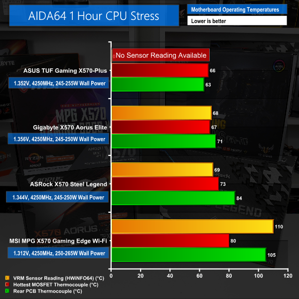
Our overclocked settings resulted in 245-250W of wall power draw under AIDA64 load. Importantly, we saw no signs of VRM-induced frequency throttling, so that’s a good result to start with.
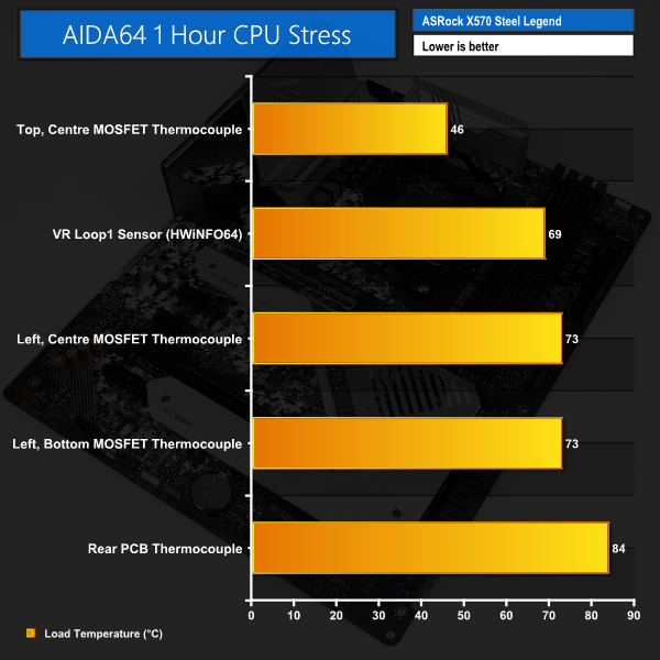
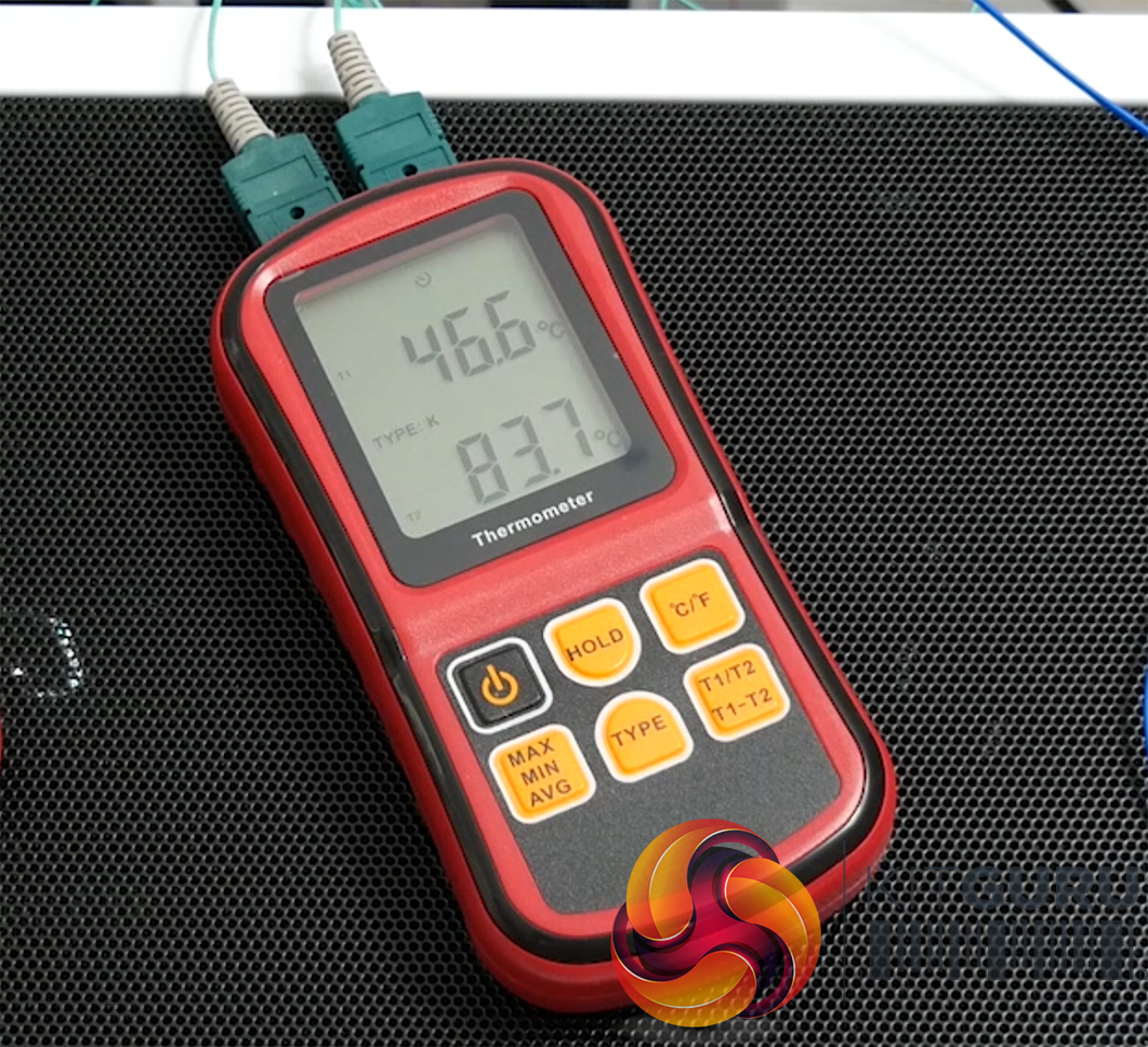
Looking at the MOSFET temperature performance, we saw a maximum temperature of 73°C, when normalised to 25°C ambient. This highest temperature reading was actually displayed on both the bottom- and middle-mounted power stages in ASRock’s configuration, which is a little surprising at first. It then becomes clear why the central power stage is operating at the same temperature as the end power stage – ASRock puts the entire bank of eight phases feeding the CPU to the left of the motherboard and underneath the single 82 gram heatsink. 1 hour is long enough to reach thermal steady state and the nearby MOSFETs operate at the same temperature.
73°C is hot but it is no real cause for concern. According to ASRock’s software-based sensor reading, the motherboard VR Loop1 sensor showed 69°C, so this reading is not too far away from our direct measurement, which is good.
Our thermocouple mounted on the top-side bank of MOSFETs above the AM4 socket highlighted that the SoC doesn’t get pushed particularly hard for CPU-only loads. The reading stayed below 50°C throughout testing. This does, however, highlight some degree of inefficiency with ASRock’s power delivery layout. Two of the eight CPU power phases could have been shifted to this region so that their heat load could be placed on the secondary heatsink. Perhaps this is not deemed an issue as the recorded temperature levels were fine anyway.
The rear PCB recorded temperature was high at just under 85°C. That’s pretty hot for a motherboard PCB. Clearly, a significant amount of thermal energy is soaking into the motherboard PCB rather than through the heatsink. A better heatsink design and more efficient physical distribution of the MOSFET power stages would have compensated for this.
We also noticed that the top side power stage temperature rose by a couple of degrees when the system was powered down and airflow was removed. This implies that heat from the PCB is soaking into the top VRM heatsink and causing a rise in MOSFET temperature, even if it is only for a few minutes before starting to cool again. Thankfully, the PCB temperature drops quite quickly once load is removed, however, that may not be the case if a heavy GPU or X570 chipset load has been applied in tandem.
After five minutes of the load being removed on system shut down, the CPU-side power stages cooled to just over 50°C while the PCB was just under 50°C. This is a decent cooling rate and shows that the heatsink can flush away its thermal load even if the system is shut down quickly after a heavy load.
Overall, we would say that there is no cause for concern from ASRock’s X570 Steel Legend. The relatively small heatsink does a decent enough job at dealing with the efficient 8-phase power delivery system. PCB temperatures are pretty high, but this did not result in instability or worrying temperature sensor readings. We saw no signs of instability at all throughout testing.
ASUS TUF Gaming X570-Plus Wi-Fi
Moving on to ASUS’ TUF Gaming X570-Plus, we see the first of our twelve physical CPU VCore VRM solutions.
Our overclocked settings resulted in power draw that was practically identical to that of ASRock’s board at 245-255W under AIDA loading. We did not see any signs of VRM-induced CPU clock speed throttling.
Annoyingly, ASUS does not include data for VRM temperature sensor readings through software tools. This is despite the SiC639 DrMOS power stages featuring thermal monitoring capabilities. As such, we cannot make a comparison between our measured results and the software readings.
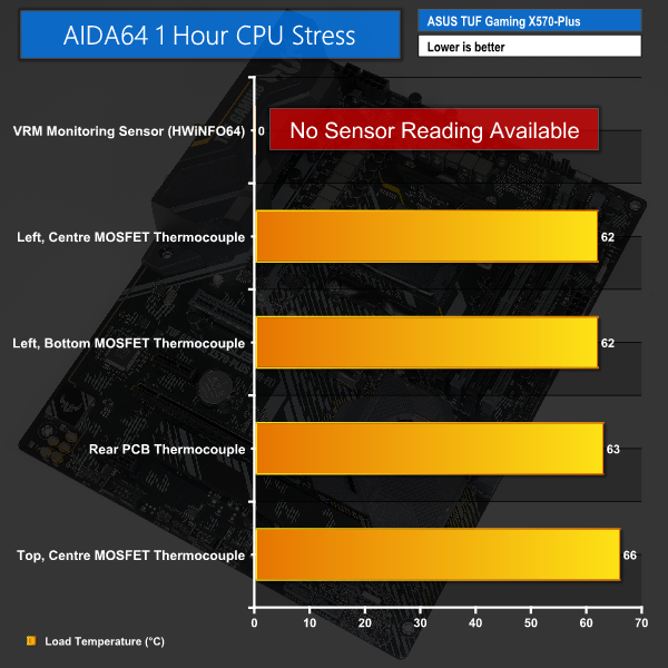
Looking at the MOSFET temperature performance, we saw a maximum temperature of 66°C, when normalised to 25°C ambient. Unsurprisingly, the highest temperature reading was displayed by the central power stage mounted above the CPU socket, beneath the small VRM heatsink. The central and lowest power stages mounted to the left of the CPU socket, beneath the larger cooler, operated around 4°C cooler at 62°C.
A maximum temperature of less than 70°C when mounted under ASUS’ anaemic heatsinks is a good result and speaks volumes about the TUF X570-Plus’ VRM solution. Balancing a hefty CPU load pushing close to 200W across twelve physical VRM phases allows the load per phase to be reduced, compared to lesser phase count solutions. This translates into solid operating temperatures, according to our results. As we also saw with ASRock’s board, the Vishay DrMOS power stages do a good job for this level of load.
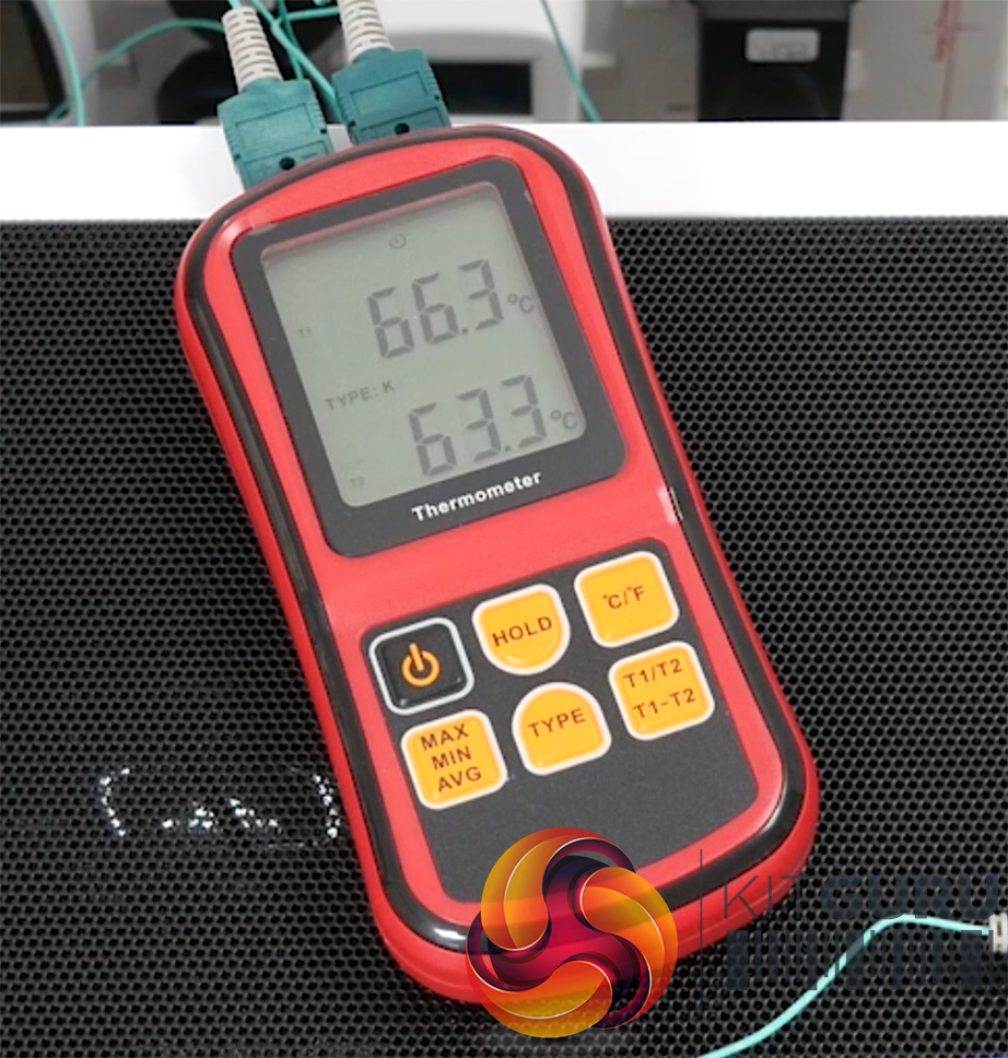
The rear PCB temperature, measured beneath the central MOSFET from the left-side bank, hit a maximum of 63°C when normalised to 25°C ambient. ASUS’ six-layer PCB looks to be handling heat soak from the MOSFETs well, as the PCB temperature is absolutely no cause for concern.
Also aided by the six-layer PCB is the cooling rate directly after load removal and system shut down. After five minutes, the MOSFETs were down to the mid-40s and the PCB cooled even quicker by dropping just below 40°C in this time period.
Overall, ASUS looks to have deployed a well-built power delivery solution on the TUF Gaming X570-Plus motherboard. Despite using a twelve-phase design that is only driven by four real phases without doublers, ASUS’ solution is clearly well-built for the heavy heat loads placed on it by an overclocked Ryzen 9 12-core chip.
Gigabyte X570 Aorus Elite
Now looking at Gigabyte’s X570 Aorus Elite, we see the other twelve phase competitor at this price point, albeit with a different method of delivering those dozen CPU power delivery phases.
Our overclocked settings resulted in power draw that was very close to that of ASRock’s and ASUS’ competitors at around 245W.
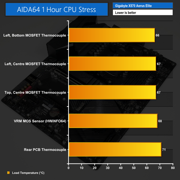
We recorded a maximum temperature on the Vishay SiC634 DrMOS power stages of 67°C, when normalised to 25°C ambient. Comparing the data between our sensors, it is clear that Gigabyte’s mounting distribution of the power phases and VRM heatsinks is smart, as there was never more than a 1°C difference between the left-side power stages and the top-side ones.
Comparing our recorded data to that of the ITE chipset-based VR MOS sensor that feeds data to software such as HWiNFO64, sensor readings of 68°C imply good accuracy and relevant data that users can trust without needing to break out the thermocouples.
As was the case with ASUS’ TUF X570-Plus, a maximum recorded temperature below 70°C is a strong result for an affordable X570 motherboard handling an overclocked 12-core CPU.
The rear PCB temperature peaked at just over 70°C. This is a decent enough result, especially when Gigabyte’s use of a lower-cost 4-layer PCB is factored in.
The cooling rate was also perfectly good, with the MOSFET sensors and PCB sensor showing readings of less than 60°C after just 1 minute of load removal.
Overall, Gigabyte’s power delivery solution on the X570 Aorus Elite looks to be very well-specced and the component distribution is smart. The heatsinks are good enough at keeping the Vishay power stages at healthy operating temperatures.
MSI MPG X570 Gaming Edge WiFi
MSI’s MPG X570 Gaming Edge Wi-Fi uses an eight-phase CPU power delivery system, just like ASRock. However, it is the only board in our comparison that opts for the cheaper On Semi discrete MOSFETs rather than Vishay DrMOS power stages.
As already mentioned, we had issues trying to get the wall power draw from the MSI board to comparable levels when overclocked. As such, our wall power draw for the MSI competitor was 250-265W, though it generally stayed between 250-260W.
Another challenge with testing the MSI board is that our thermocouples were experiencing significantly higher levels of EMI than with the competing solutions. This forced us to use a tactic of quickly killing system power directly after heavy load in order to record the MOSFET temperatures without EMI.
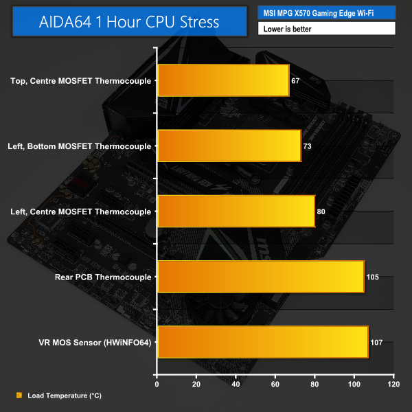
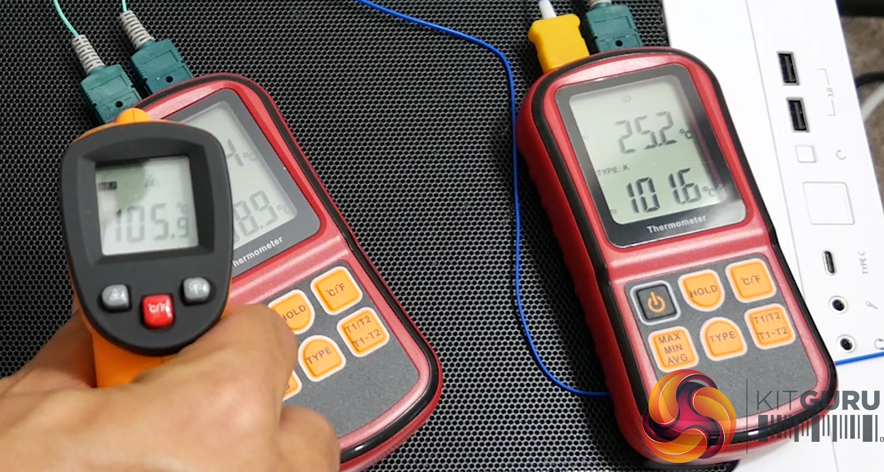
We recorded a maximum temperature of 80°C with our thermocouple mounted on the left-side, centre MOSFETs. One challenge with this reading was that our thermocouple could sometimes bridge across the high- and low-side MOSFETs as this board was particularly difficult when installing the thermocouples. Nevertheless, 80°C reading from our thermocouple is undeniably high.
Interestingly, the left-side, bottom MOSFET actually ran around 7°C cooler at 73°C. The top-side MOSFET also ran cooler at 67°C, when normalised to 25°C ambient. The difference in recorded temperature between the centre and bottom MOSFETs on the left side of the CPU socket implies that the centre one is having difficulty in shedding its heat.
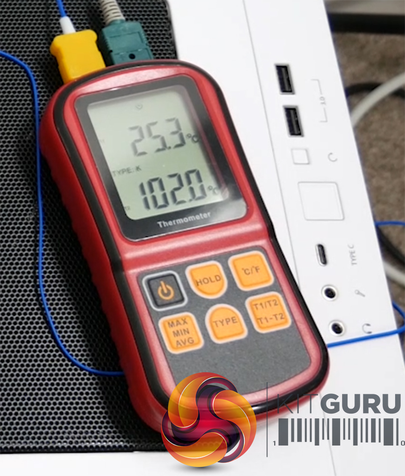
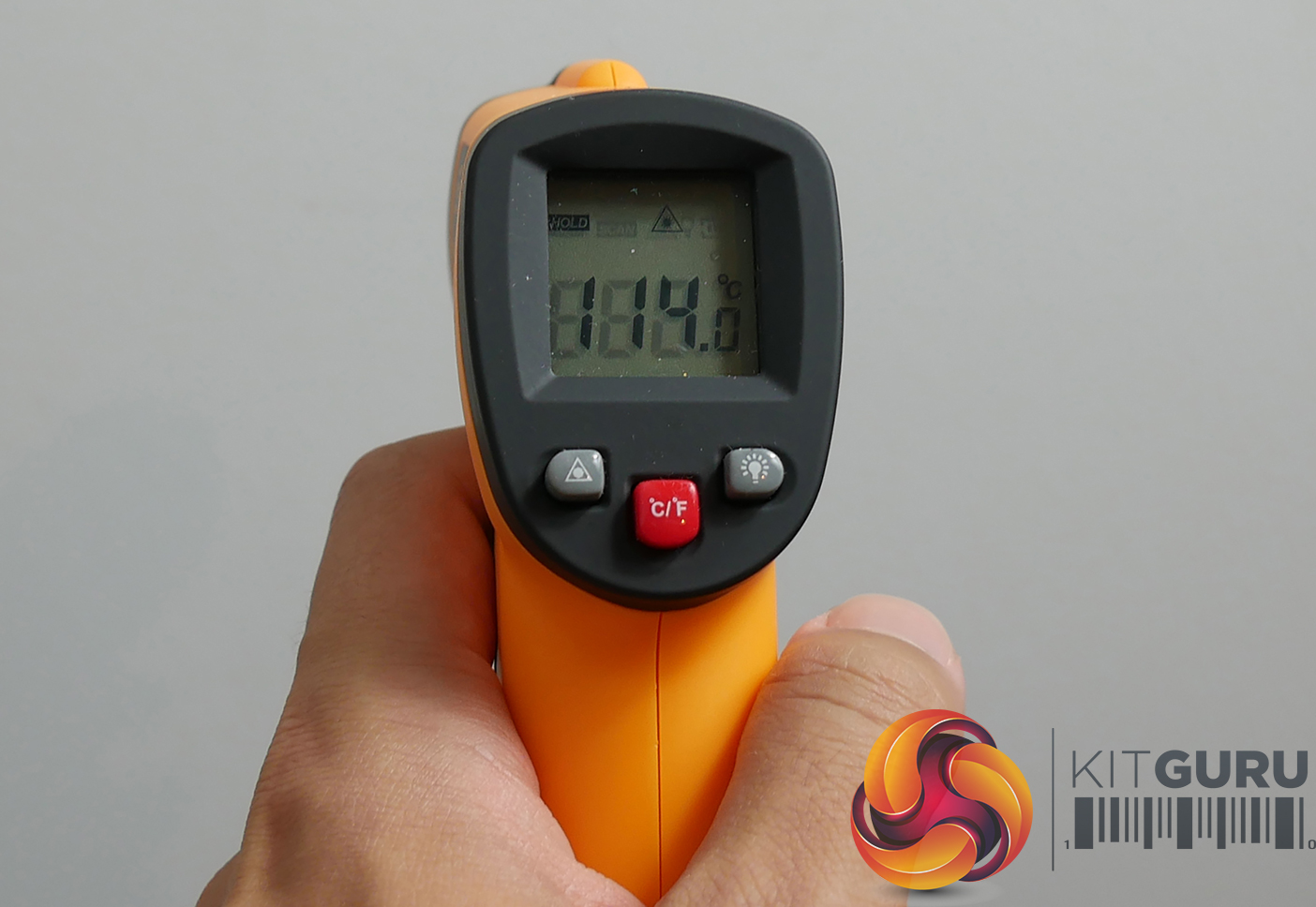
It doesn’t take us long to find the source of that difficulty in shedding heat – the PCB temperature. Topping out at more than 105°C on our thermocouple (we actually read as high as 114°C in certain spots with the laser thermometer), the PCB temperature anywhere near the MOSFETs was ridiculous. We wanted to make sure these alarming readings were correct, so an additional thermocouple was mounted on the front side PCB, to the right of the inductors. Its reading was 100°C also, so we were confident in the results.
To say that a PCB temperature of more than 100°C is alarming is an understatement. With this temperature level, I would not feel comfortable running this kind of workload on a frequent basis. Also bear in mind that there was no GPU, M.2 SSD, or X570 chipset load dumping additional heat into the motherboard PCB.
Checking the sensors from the IR PWM controller and a Nuvoton monitoring chipset in HWiNFO64 highlighted readings of just under 110°C in both cases. While the MOSFETs may technically be able to operate at these temperatures, the levels certainly aren’t good for longevity or peace of mind (which is important when building a system).
Considering that running temperatures over 100°C were highlighted by the International Rectifiers and Nuvoton sensors built into MSI’s motherboard, in addition to our own PCB readings in several locations using a laser thermometer and K-type thermocouples, we’re more than happy to believe those. The difficulties that we had with EMI and correct mounting of our thermocouples on top of the MOSFETs imply that our recorded MOSFET temperatures are possibly lower than the actual temperatures.
MSI’s power delivery solution on this motherboard is not well equipped for handling an overclocked 12-core Ryzen part. That’s disappointing, especially when its competitors all fare so well.
At least the cooling rate from MSI’s massive heatsink was a positive – the MOSFETs and PCB dropped to around 50°C five minutes after the load was removed, and with no system airflow.
Results Comparison
When it comes to raw MOSFET temperatures, ASUS and Gigabyte put in the best displays in our testing. There is little between these two solutions, though ASUS did display slightly better temperatures for the left-side MOSFETs thanks to its CPU VCore VRM and heatsink distribution. The PCB temperatures were also a little better for ASUS thanks to its use of a six-layer PCB compared to Gigabyte’s four-layer.
Despite the ASUS board offering marginally better temperatures for the MOSFETs overall, the accurate in-built temperature sensor for Gigabyte’s X570 Aorus Elite was a clear positive. It is a shame that ASUS’ motherboard does not display VRM temperature readings in OS-based monitoring software. Based on our testing, ASUS shows excellent performance and has absolutely nothing to hide.
ASRock’s X570 Steel Legend displayed solid performance from its lower-cost eight-phase CPU VCore VRM. The MOSFET temperatures were higher than ASUS’ and Gigabyte’s but the margin was no cause for concern. ASRock’s board also featured a VRM temperature sensor reading in monitoring software which proved to have a reasonable degree of accuracy in our testing. One area where ASRock was not as competitive as the ASUS and Gigabyte alternatives was with PCB temperature. This is likely due to the deployment of all eight CPU VCore power delivery phases to the left of the AM4 socket, thus resulting in more localised heating that is increasingly difficult to conduct and dissipate from the PCB.
One clear area where ASRock’s X570 Steel Legend has benefits is to APU users. The two-phase SoC VRM gets its own dedicated heatsink and maintains the use of Vishay DrMOS power stages. Users looking to push an APU hard may be interested by this design choice on ASRock’s part.
MSI’s MPG X570 Gaming Edge WiFi did not perform well in our testing, even despite the conservative MOSFET temperature readings that we gathered due to our testing difficulties. Recorded MOSFET temperatures of 80°C, with sensor readings suggesting 110°C, are not good for worry-free computing. The PCB temperatures were too high to run this type of current draw on a high-powered Ryzen CPU for extended periods of time.
MSI aimed to brute force a large heatsink onto its motherboard to compensate for the use of more basic power delivery components. But according to the temperature data that we recorded, this was not a reasonable design choice for a motherboard that costs more than £200. While we did not see any VRM-induced CPU throttling in our test runs, I would not feel confident running my system day-to-day knowing that the PCB is hitting more than 100°C with relative ease. We were fortunate enough to have decent case airflow in our testing, also, which is not always the available to many users.
So, there we have it. ASUS' TUF Gaming X570-Plus and Gigabyte's X570 Aorus Elite both do well with their twelve-phase deployments, with ASUS operating a little cooler on average but forcing users to give up OS-based software readings as a compromise. The granularity of Gigabyte's six control phases in a doubled configuration may also prove beneficial in scenarios outside of heavy, all-out load. Both of these motherboards will be excellent choices at this £210 price point.
ASRock’s X570 Steel Legend delivered solid results from its eight-phase CPU VCore system, despite running hotter than ASUS and Gigabyte on average. Users running an APU and wanting to push the SoC VRM hard may be interested in ASRock’s solution as the two-phase system uses strong DrMOS power stages and is given an entire heatsink to itself.
MSI’s MPG X570 Gaming Edge WiFi uses basic MOSFETs and tries to use brute force to cool them – but this doesn’t work very well, with sensor-reported temperatures as high as 110°C and physical PCB readings showing more than 100°C. I wouldn’t recommend this board for use with an overclocked Ryzen 12-core or 16-core CPU. That said, it’s likely to be fine for lower-powered parts, which is a good thing as I have previously recommended this exact model for a friend's Ryzen 7 3700X build.
![]()
You can purchase these roughly £210 X570 motherboards at Overclockers UK.
KitGuru says: The 12-core Ryzen 9 3900X processor delivers extreme performance from a mainstream part but it does so while pushing motherboard power delivery systems hard. As such, it is good to see that there are motherboards at this affordable – by X570 standards – price point with the capacity to drive the overclocked brute.